LTC5588-1
PIN FUNCTIONS
EN (Pin 1): Enable Input. When the enable pin voltage is
higher than 2V, the IC is on. When the input voltage is less
than 1V, the IC is off.
LINOPT (Pin 7): Linearity Optimization Input. An external
voltage can be applied to this pin to optimize the linearity
(OIP3)underaspecificapplicationcondition. Itsoptimum
voltagedependsontheLOfrequency,temperature,supply
voltage, baseband frequency and signal bandwidth. The
typical input voltage range is from 2V to 3.7V. The pin can
be left floating for good overall linearity performance.
GND (Pins 2, 5, 8, 11, 12, 14, 17, 19, 20, 23, Exposed
Pad Pins 25 and 26): Ground. Pins 2, 5, 8, 11, 20, 23
and exposed pad Pin 25 (group 1) are connected together
internallywhilePins12,14,17,19andexposedpadPin 26
(group 2) are tied together and serve as the ground return
for the RF balun. For best overall performance all ground
pins should be connected to RF ground. For best OIP2
performance it is recommended to connect group 1 and
group 2 only at second and lower level ground layers
of the PCB, not the top layer. A thermistor (temperature
BBMQ,BBPQ(Pins9,10):BasebandInputsoftheQChan-
nel. The input impedance of each input is about –3kΩ. It
should be externally biased to a 0.5V common mode level.
Do not apply common mode voltage beyond 0.55V .
DC
RF (Pin 16): RF Output. The RF output is a DC-coupled
single-ended output with 50Ω output impedance at RF
frequencies.AnAC-couplingcapacitorof6.2pF(C7),should
be used at this pin for 0.7GHz to 3.5GHz operation.
variable resistor) of 1.4kΩ at 25°C and V = 3.3V with
CC
temperature coefficient of 11Ω/°C is connected between
group 1 and group 2.
V
,V (Pins24,18):PowerSupply.Itisrecommended
CC1 CC2
LOP (Pin 3): Positive LO Input. An AC-coupling capacitor
(1nF) in series with 50Ω to ground provides the best OIP2
performance.
to use 2 × 1nF and 2 × 4.7μF capacitors for decoupling to
ground on these pins.
BBPI, BBMI (Pins 21, 22): Baseband Inputs of the
I Channel. The input impedance of each input is about
–3kΩ. It should be externally biased to a 0.5V common
mode level. Do not apply common mode voltage beyond
LOM (Pin 4): Negative LO Input. An AC-coupled 50Ω LO
signal source can be applied to this pin.
NC (Pins 6, 13, 15): No Electrical Connection.
0.55V .
DC
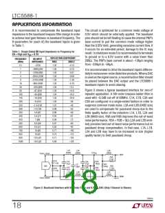
BLOCK DIAGRAM
V
V
GND
23
NC
CC1 CC2
20
25
24
18
13
15
BBPI 21
BBMI 22
VqI
I CHANNEL
16 RF
0°
90°
GND
BBPQ 10
1
EN
VqI
Q CHANNEL
BBMQ
9
2
5
8
11
3
4
6
7
12 14 17 19 26
GND
LOP LOM NC LINOPT
GNDRF
55881 BD
55881fb
16

 Linear [ Linear ]