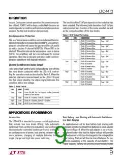
LTC4413
U
OPERATIO
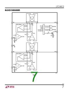
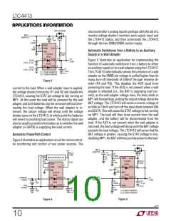
The LTC4413 is described with the aid of the Block
Diagram (Figure 1). Operation begins when the power
source at VINA or VINB rises above the undervoltage
lockout (UVLO) voltage of 2.4V and either of the ENBA or
ENBB control pins is low. If only the voltage at the VINA pin
is present, the power source to the LTC4413 (VDD) will be
supplied from the VINA pin. The amplifier (A) will pull a
current proportional to the difference between VINA and
VOUTA from the gate (VGATEA) of the internal PFET (PA),
driving this gate voltage below VINA. This will turn on PA.
As VOUTA is pulled up to a forward voltage drop (VFWD) of
20mV below VINA, the LTC4413 will regulate VGATEA to
maintain the small forward voltage drop. The system is
now in forward regulation and the load at VOUTA will be
powered from the supply at VINA. As the load current
varies, VGATEA will be controlled to maintain VFWD until the
load current exceeds the transistor’s (PA) ability to deliver
the current as VGATEA approaches GND. At this point the
PFET will behave as a fixed resistor with resistance RON,
whereby the forward voltage will increase slightly with
increasedloadcurrent.AsthemagnitudeofIOUT increases
further(suchthatILOAD >IOC),theLTC4413willfixtheload
current to the constant value IOC to protect the device. The
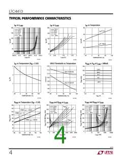
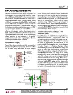
characteristics for parameters RFWD, RON, VFWD and IOC
are specified with the aid of Figure 2, illustrating the
LTC4413 forward voltage drop versus that of a Schottky
diode.
If another supply is provided at VINB, the LTC4413 will
likewise regulate the gate voltage on PB to maintain the
output voltage VOUTB just below the input voltage VINB. If
thisalternatesupply, VINB, exceedsthevoltageatVINA, the
LTC4413 will select this input voltage as the internal
supply (VDD). This second ideal diode operates indepen-
dently of the first ideal diode function.
When an alternate power source is connected to the load
at VOUTA (or VOUTB), the LTC4413 will sense the increased
voltage at VOUTA and amplifier A will increase the voltage
V
GATEA, reducing the current through PA. When VOUTA is
higher than VINA + VRTO, VGATEA will be pulled up to VDD,
which will turn off PA. The internal power source for the
LTC4413 (VDD) will then be diverted to source current
from the VOUTA pin, only if VOUTA is larger than VINB (or
VOUTB). The system is now in the reverse turn-off mode.
Power to the load is being delivered from an alternate
supply and only a small current is drawn from VINA to
sense the potential at VINA
.
When the selected channel of the LTC4413 is in reverse
turn-off mode or both channels are disabled, the STAT pin
will sink 9µA of current (ISON) if connected.
Channel selection is accomplished using the two ENB
pins, ENBA and ENBB. When the ENBA input is asserted
(high), PA will have its gate voltage pulled to VDD at a
controlled rate, limiting the turn-off time to avoid voltage
spiking at the input when being driven by an inductive
source impedance. A 3µA pull-down current on the ENB
pins will ensure a low level at these inputs if left floating.
I
OC
SLOPE
1/R
ON
I
FWD
Overcurrent and Short-Circuit Protection
LTC4413
During an overcurrent condition, the output voltage will
droop as the load current exceeds the amount of current
that the LTC4413 can supply. At the time when an over-
current condition is first detected, the LTC4413 will take
some time to detect this condition before reducing the
current to IMAX. For short durations after the output is
shorted, the current may exceed IMAX. The magnitude of
this peak short-circuit current can be large, depending on
the load current immediately before the short circuit
SCHOTTKY
DIODE
SLOPE
1/R
FWD
0
0
FORWARD VOLTAGE (V)
4413 F02
Figure 2
4413f
8

 Linear [ Linear ]