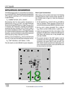
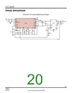
LTC3649
APPLICATIONS INFORMATION
The initial output voltage step may not be within the band-
width of the feedback loop, so the standard second order
overshoot/DC ratio cannot be used to determine phase
through the SW pin. Depending on the size of the output
capacitorandtheresistivityoftheshort, highcurrentsmay
flow through the internal body diode, and cause damage
margin. The gain of the loop increases with the R and
to the part. If a V discharge is possible, preventative
ITH
IN
thebandwidthoftheloopincreaseswithdecreasingC .If
measures should be taken to prevent current flow through
the internal body diode. Simple solutions would be plac-
ing a Schottky diode in series with the supply (Figure 3),
ITH
R
isincreasedbythesamefactorthatC isdecreased,
ITH
ITH
the zero frequency will be kept the same, thereby keeping
the phase the same in most critical frequency ranges of
the feedback loop.
or placing a Schottky diode from V
to V (Figure 4).
OUT
IN
Output Short Considerations
Theoutputvoltagesettlingbehaviorisrelatedtothestability
of the closed-loop system and will demonstrate the actual
overall supply performance. For a detailed explanation of
optimizing the compensation components, including a
review of control loop theory, refer to Linear Technology
Application Note 76.
In an event where the output of the LTC3649 is shorted
to GND through a low resistance, high inductance trace/
wire, it is likely for the output voltage to momentarily drop
below GND. In a typical application where the output is
tied directly to the V
pin, it would violate the ABSMAX
OUT
specification of the pin and potentially cause damage to
the IC. To prevent damage in this case, connect a 100Ω
Insomeapplications,amoreseveretransientcanbecaused
by switching in loads with large (>10µF) input capacitors.
Thedischargedinputcapacitorsareeffectivelyputinparal-
resistor between the output and the V
pin.
OUT
lel with C , causing a rapid drop in V . No regulator
OUT
OUT
Efficiency Considerations
can deliver enough current to prevent this problem if the
switchconnectingtheloadhaslowresistanceandisdriven
quickly. The solution is to limit the turn-on speed of the
load switch driver. A hot swap controller is designed spe-
cifically for this purpose and usually incorporates current
limiting, short-circuit protection, and soft-start operation.
The percent efficiency of a switching regulator is equal to
the output power divided by the input power times 1008.
It is often useful to analyze individual power losses to de-
termine what is limiting the efficiency and which change
would produce the most improvement. Percent efficiency
can be expressed as:
Input Disconnect/Input Short Considerations
8 Efficiency = 1008 – (P1 + P2 + P3 +…)
If at any point the input supply is removed with the output
voltage still held high through its capacitor, power will be
drawn from the output capacitor to power the chip, until
whereP1,P2,etc.aretheindividuallossesasapercentage
of input power. Although all dissipative elements in the
circuitproducelosses,threemainsourcesusuallyaccount
2
the output voltage drops below the minimum V require-
IN
for most of the losses in LTC3649 circuits: 1) I R losses,
ments of the chip.
2) switching and biasing losses, 3) other losses.
However, if the V pin is grounded while the output is
IN
held high, regardless of the RUN state, parasitic body
diodesinsidetheLTC3649willpullcurrentfromtheoutput
L
V
V
SW
LTC3649
V
OUT
V
IN
V
IN
IN
IN
LTC3649
C
C
OUT
47µF
C
IN
IN
22µF
22µF
3649 F03
3649 F04
Figure 3. Schottky Diode in Series with the Supply
Figure 4. Schottky Diode from VOUT to VIN
3649fb
16
For more information www.linear.com/LTC3649

 Linear [ Linear ]