LTC3649
APPLICATIONS INFORMATION
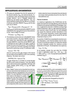
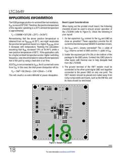
Board Layout Considerations
TheFE2ꢀpackagejunction-to-ambientthermalresistance,
θ ,isaround30°C/W.Therefore,thejunctiontemperature
JA
When laying out the printed circuit board, the following
checklist should be used to ensure proper operation of
the LTC3649 (refer to Figure 5). Check the following in
your layout:
of the regulator operating in a 25°C ambient temperature
is approximately:
T = 0.99ꢀW • 30°C/W + 25°C = 54.94°C
J
1. Do the capacitors C connect to the V and GND as
Remembering that the above junction temperature is
IN
IN
close as possible? These capacitors provide the AC
obtained from an R
at 25°C, we might recalculate
DS(ON)
currenttotheinternalpowerMOSFETsandtheirdrivers.
the junction temperature based on a higher R
since
DS(ON)
it increases with temperature. Redoing the calculation
2. Are C
and L closely connected? The (–) plate of
OUT
assuming that R increased 108 at 54.94°C yields a
SW
C
returns current to GND and the (–) plate of C .
OUT
IN
new junction temperature of 60°C. If the application calls
for a higher ambient temperature and/or higher switching
frequency, careshouldbetakentoreducethetemperature
rise of the part by using a heat sink or air flow.
3. Solder the exposed pad (Pin 29) on the bottom of the
package to the GND plane. Connect this GND plane to
other layers with thermal vias to help dissipate heat
from the LTC3649.
IfEXTV isnotconnectedtoV ,theICcurrentwillcome
CC
OUT
4. The ground terminal of the ISET resistor must be
connected to the other quiet signal GND and together
connected to the power GND on only one point. The
ISET resistor should be placed and routed away from
noisy components and traces, such as the SW line, and
its trace should be minimized
from V . In this case, the total power dissipation will be:
IN
2
P = 16A • 5ꢀ.25mΩ + 24V • 20mA = 1.41W
D
This will result in an extra 400mW of power dissipation.
Figure 5. Sample PCB Layout
3649fb
18
For more information www.linear.com/LTC3649

 Linear [ Linear ]