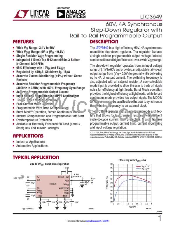
LTC3649
APPLICATIONS INFORMATION
2
1. I R losses are calculated from the DC resistances of
diodeconductionlossesduringdead-timeandinductor
core losses which generally account for less than 28
total additional loss.
the internal switches, R , and external inductor, R .
SW
L
In continuous mode, the average output current flows
through inductor L but is “chopped” between the
internal top and bottom power MOSFETs. Thus, the
series resistance looking into the SW pin is a function
Thermal Conditions
In a majority of applications, the LTC3649 does not dis-
sipatemuchheatduetoitshighefficiencyandlowthermal
resistanceofitsexposed-backQFNandFEpackages.How-
ever, in applications where the LTC3649 is running at high
of both top and bottom MOSFET R
cycle (D) as follows:
and the duty
DS(ON)
R
SW
= (R )(D) + (R )(1 – D)
DS(ON)TOP DS(ON)BOT
ambient temperature, high V , high switching frequency,
IN
TheR
forboththetopandbottomMOSFETscanbe
DS(ON)
and maximum output current load, the heat dissipated
may exceed the maximum junction temperature of the
part. If the junction temperature reaches approximately
1ꢀ0°C, both power switches will be turned off until the
temperature drops by 15°C.
obtained from the Typical Performance Characteristics
2
curves. Thus to obtain I R losses:
2
2
I R losses = I
(R + R )
SW L
OUT
2. The switching current is the sum of the MOSFET driver
and control currents. The power MOSFET driver cur-
rent results from switching the gate capacitance of
the power MOSFETs. Each time a power MOSFET gate
is switched from low to high to low again, a packet of
charge dQ moves from IN to ground. The resulting dQ/
dt is a current out of IN that is typically much larger
than the DC control bias current. In continuous mode:
To avoid the LTC3649 from exceeding the maximum junc-
tion temperature, some thermal analysis must be done.
The goal of the thermal analysis is to determine whether
the power dissipated exceeds the maximum junction
temperature of the part. The temperature rise is given by:
T
RISE
= P • θ
D JA
As an example, consider the case when the LTC3649
is used in applications where V = 24V, I = 4A,
I
= f(Q + Q )
T B
GATECHG
IN
OUT
where Q and Q are the gate charges of the internal
top and bottom power MOSFETs and f is the switching
frequency. The power loss is thus:
T
B
f = 1MHz, and V
= 3.3V. The equivalent power MOSFET
OUT
resistance R is:
SW
VOUT
V
V
IN
Switching Loss = I
• V
IN
OUT
GATECHG
RSW =RDS(ON)TOP
•
+RDS(ON)BOT • 1−
V
IN
The gate charge loss is a function of current through
the INTV pin as well as frequency. Thus, their effects
3.3V
24V
3.3V
24V
CC
= 110mΩ •
= 5ꢀ.25mΩ
+50mΩ • 1−
will be more pronounced in application with high LDO
supply voltages (either EXTV or V ) and higher
CC
IN
frequencies.
3. Other “hidden” losses such as transition loss and cop-
per trace and internal load resistances can account for
additional efficiency degradations in the overall power
system. It is very important to include these “system”
level losses in the design of a system. Transition loss
arises from the brief amount of time the top power
MOSFET spends in the saturated region during switch
node transitions. The LTC3649 internal power devices
switch quickly enough that these losses are not signifi-
cantcomparedtoothersources. Otherlossesincluding
In the case where the EXTV pin is connected to the OUT
CC
pin, the V current will be minimal as most of the current
IN
used to bias up internal circuitry and gate drive will come
directlyfromEXTV . Typicallyfora1MHzapplication, the
CC
current drawn from EXTV will be 20mA.
CC
Therefore, the total power dissipated by the part is:
2
P = I
• R + V • I
EXTVCC EXTVCC
D
OUT
SW
2
= 16A • 5ꢀ.25mΩ + 3.3V • 20mA
= 99ꢀmW
3649fb
17
For more information www.linear.com/LTC3649

 Linear [ Linear ]