LTC3649
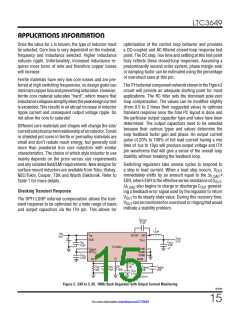
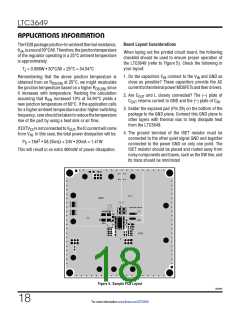
APPLICATIONS INFORMATION
5. Keep sensitive components away from the SW pin. The
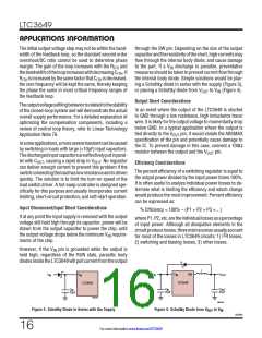
For a typical soft-start time of 2ms (08 to 908 of final
ISET resistor, R resistor, the compensation compo-
V
value), the C should be:
T
OUT
SET
nentsC andR ,andtheINTV bypasscapsshould
ITH
ITH
CC
2ms = 2.3 • R • C
SET
SET
be routed away from the SW trace and the inductor.
⇒C = ꢀ.7nF
SET
6. A ground plane is preferred.
A typical 10nF capacitor can be used for C
.
SET
7. Flood all unused areas on all layers with copper, which
reduces the temperature rise of power components.
These copper areas should be connected to GND.
Because efficiency is important at both high and low load
current, Burst Mode operation will be utilized. Select from
the characteristic curves the correct R resistor for the
T
1MHz switching frequency. Based on that, R should be
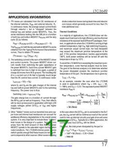
Design Example
T
100k. Then calculate the inductor value to achieve a cur-
As a design example, consider the LTC3649 in an applica-
tion with the following specifications:
rent ripple that is about 408 of the maximum load current
at maximum V :
IN
V = 24V to 36V
IN
5V
5V
36V
L =
1−
= 2.7µH
V
OUT
= 5V
1MHz •1.6A
I
I
f
= 4A
= 500mA
= 1MHz
OUT(MAX)
OUT(MIN)
C
OUT
will be selected based on the ESR that is required
to satisfy the output ripple requirement and the bulk ca-
pacitance needed for loop stability. For this design, two
47µF ceramic capacitors will be used.
SW
First, the R is selected based on:
SET
VOUT
50µA 50µA
5V
C should be sized for a maximum current rating of:
IN
RSET
=
=
= 100kΩ
1/2
5V 36V
IRMS = 4A
−1 = 1.3ꢀA
For best accuracy, 0.58 100k resistor is selected.
36V 5V
Decoupling the V pin with one 22µF ceramic capacitor
IN
is adequate for most applications.
3649fb
19
For more information www.linear.com/LTC3649

 Linear [ Linear ]