LTC3633A/LTC3633A-1
APPLICATIONS INFORMATION
Internal/External Loop Compensation
margin and/or damping factor can be estimated using the
percentage of overshoot seen at this pin.
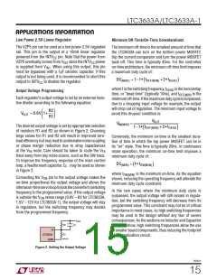
The LTC3633A provides the option to use a fixed internal
loop compensation network to reduce both the required
external component count and design time. The internal
loop compensation network can be selected by connect-
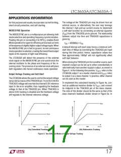
The ITH external components shown in Figure 3 circuit
will provide an adequate starting point for most applica-
tions. The series R-C filter sets the dominant pole-zero
loop compensation. The values can be modified slightly
(from 0.5 to 2 times their suggested values) to optimize
transient response once the final PC layout is done and
the particular output capacitor type and value have been
determined. The output capacitors need to be selected
because their various types and values determine the
loop gain and phase. An output current pulse of 20% to
100% of full load current having a rise time of ~1μs will
produce output voltage and ITH pin waveforms that will
give a sense of the overall loop stability without breaking
the feedback loop.
ing the ITH pin to the INTV pin. To ensure stability it is
CC
recommendedthatinternalcompensationonlybeusedwith
applications with f > 1MHz. Alternatively, the user may
SW
choose specific external loop compensation components
to optimize the main control loop transient response as
desired. External loop compensation is chosen by simply
connecting the desired network to the ITH pin.
Suggestedcompensationcomponentvaluesareshownin
Figure 3. For a 2MHz application, an R-C network of 220pF
and 13kΩ provides a good starting point. The bandwidth
of the loop increases with decreasing C. If R is increased
by the same factor that C is decreased, the zero frequency
will be kept the same, thereby keeping the phase the same
in the most critical frequency range of the feedback loop.
A 10pF bypass capacitor on the ITH pin is recommended
for the purposes of filtering out high frequency coupling
from stray board capacitance. In addition, a feedforward
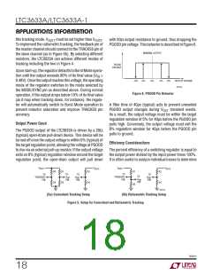
Switching regulators take several cycles to respond to a
step in load current. When a load step occurs, V
im-
OUT
•ESR,where
mediatelyshiftsbyanamountequaltoΔI
LOAD
ESR is the effective series resistance of C . ΔI
also
OUT
LOAD
begins to charge or discharge C
generating a feedback
OUT
error signal used by the regulator to return V
to its
can
OUT
steady-state value. During this recovery time, V
capacitor C can be added to improve the high frequency
F
OUT
response, as previously shown in Figure 2. Capacitor C
be monitored for overshoot or ringing that would indicate
a stability problem.
F
provides phase lead by creating a high frequency zero
with R2 which improves the phase margin.
When observing the response of V
to a load step, the
OUT
initialoutputvoltagestepmaynotbewithinthebandwidth
of the feedback loop, so the standard second order over-
shoot/DCratiocannotbeusedtodeterminephasemargin.
Theoutputvoltagesettlingbehaviorisrelatedtothestability
of the closed-loop system and will demonstrate the actual
overall supply performance. For a detailed explanation of
optimizing the compensation components, including a
review of control loop theory, refer to Linear Technology
Application Note 76.
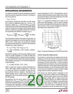
ITH
R
COMP
13k
LTC3633A
SGND
C
COMP
220pF
3633a F03
Figure 3. Compensation Component
Checking Transient Response
The regulator loop response can be checked by observing
theresponseofthesystemtoaloadstep.Whenconfigured
for external compensation, the availability of the ITH pin
not only allows optimization of the control loop behavior
butalsoprovidesaDC-coupledandACfilteredclosedloop
response test point. The DC step, rise time, and settling
behavioratthistestpointreflecttheclosedloopresponse.
Assuming a predominantly second order system, phase
Insomeapplications,amoreseveretransientcanbecaused
by switching in loads with large (>10μF) input capacitors.
Thedischargedinputcapacitorsareeffectivelyputinparal-
lel with C , causing a rapid drop in V . No regulator
OUT
OUT
can deliver enough current to prevent this problem, if the
switchconnectingtheloadhaslowresistanceandisdriven
quickly.Thesolutionistolimittheturn-onspeedoftheload
switchdriver.Ahotswapcontrollerisdesignedspecifically
3633a1f
16

 Linear [ Linear ]