LTC3633A/LTC3633A-1
APPLICATIONS INFORMATION
what is limiting the efficiency and which change would
produce the most improvement. Percent efficiency can
be expressed as:
To calculate the total power loss from the LDO load,
simply add the gate charge current and quiescent cur-
rent and multiply by V :
IN
% Efficiency = 100% – (L1 + L2 + L3 +…)
P
= (I + I ) • V
GATECHG Q IN
LDO
where L1, L2, etc. are the individual losses as a percent-
age of input power.
3. Other “hidden” losses such as transition loss, cop-
per trace resistances, and internal load currents can
account for additional efficiency degradations in the
overall power system. Transition loss arises from the
brief amount of time the top power MOSFET spends
in the saturated region during switch node transitions.
The LTC3633A internal power devices switch quickly
enough that these losses are not significant compared
to other sources.
Although all dissipative elements in the circuit produce
losses, three main sources usually account for most of
2
the losses in LTC3633A circuits: 1) I R losses, 2) switch-
ing losses and quiescent power loss 3) transition losses
and other losses.
2
1. I R losses are calculated from the DC resistances of
the internal switches, R , and external inductor, R .
SW
L
Other losses, including diode conduction losses during
dead-time and inductor core losses, generally account
for less than 2% total additional loss.
In continuous mode, the average output current flows
through inductor L but is “chopped” between the
internal top and bottom power MOSFETs. Thus, the
series resistance looking into the SW pin is a function
Thermal Considerations
of both top and bottom MOSFET R
cycle (DC) as follows:
and the duty
DS(ON)
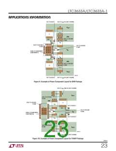
The LTC3633A requires the exposed package backplane
metal (PGND) to be well soldered to the PC board to
provide good thermal contact. This gives the QFN and
TSSOP packages exceptional thermal properties, which
are necessary to prevent excessive self-heating of the part
in normal operation.
R
= (R )(DC) + (R )(1 – DC)
DS(ON)TOP DS(ON)BOT
SW
TheR
forboththetopandbottomMOSFETscanbe
DS(ON)
obtained from the Typical Performance Characteristics
2
curves. Thus to obtain I R losses:
2
2
I R losses = I
(R + R )
In a majority of applications, the LTC3633A does not dis-
sipatemuchheatduetoitshighefficiencyandlowthermal
resistance of its exposed-back QFN package. However, in
applications where the LTC3633A is running at high ambi-
OUT
SW
L
2. The internal LDO supplies the power to the INTV rail.
CC
The total power loss here is the sum of the switching
losses and quiescent current losses from the control
circuitry.
ent temperature, high V , high switching frequency, and
IN
maximum output current load, the heat dissipated may
exceed the maximum junction temperature of the part. If
the junction temperature reaches approximately 150°C,
both power switches will be turned off until temperature
returns to 140°C.
Each time a power MOSFET gate is switched from low
to high to low again, a packet of charge dQ moves from
V
to ground. The resulting dQ/dt is a current out of
IN
INTV that is typically much larger than the DC control
CC
biascurrent.Incontinuousmode,I
=f(Q +Q ),
GATECHG
T B
To prevent the LTC3633A from exceeding the maximum
junction temperature of 125°C, the user will need to do
some thermal analysis. The goal of the thermal analysis
where Q and Q are the gate charges of the internal
T
B
top and bottom power MOSFETs and f is the switching
frequency. For estimation purposes, (Q + Q ) on each
T
B
LTC3633A regulator channel is approximately 2.3nC.
3633a1f
19

 Linear [ Linear ]