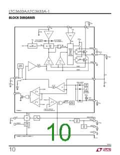
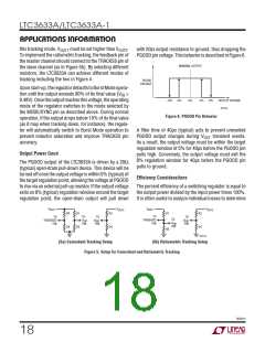
LTC3633A/LTC3633A-1
APPLICATIONS INFORMATION
Several capacitors may also be paralleled to meet size or
height requirements in the design. For low input voltage
applications, sufficient bulk input capacitance is needed
to minimize transient effects during output load changes.
EventhoughtheLTC3633Adesignincludesanovervoltage
protection circuit, care must always be taken to ensure
inputvoltagetransientsdonotposeanovervoltagehazard
to the part.
rating and low ESR make them ideal for switching regula-
tor applications. However, due to the self-resonant and
high-Q characteristics of some types of ceramic capaci-
tors, care must be taken when these capacitors are used
at the input. When a ceramic capacitor is used at the input
and the power is supplied by a wall adapter through long
wires, a load step at the output can induce ringing at the
V input. At best, this ringing can couple to the output and
IN
be mistaken as loop instability. At worst, a sudden inrush
The selection of C
is determined by the effective series
OUT
of current through the long wires can potentially cause a
resistance(ESR)thatisrequiredtominimizevoltageripple
and load step transients as well as the amount of bulk
capacitance that is necessary to ensure that the control
loop is stable. Loop stability can be checked by viewing
voltage spike at V large enough to damage the part. For
IN
a more detailed discussion, refer to Application Note 88.
When choosing the input and output ceramic capacitors,
choose the X5R and X7R dielectric formulations. These
dielectrics have the best temperature and voltage charac-
teristics of all the ceramics for a given value and size.
the load transient response. The output ripple, ΔV , is
approximated by:
OUT
⎛
⎞
⎟
⎠
1
ΔVOUT < ΔI ESR+
⎜
⎝
L
8 • f • COUT
INTV Regulator Bypass Capacitor
CC
An internal low dropout (LDO) regulator draws power
When using low-ESR ceramic capacitors, it is more useful
tochoosetheoutputcapacitorvaluetofulfillachargestor-
age requirement. During a load step, the output capacitor
mustinstantaneouslysupplythecurrenttosupporttheload
until the feedback loop raises the switch current enough
to support the load. The time required for the feedback
looptorespondisdependentonthecompensationandthe
output capacitor size. Typically, 3 to 4 cycles are required
to respond to a load step, but only in the first cycle does
from the V input and produces the 3.3V supply that
IN1
powers the internal bias circuitry and drives the gate of
the internal MOSFET switches. The INTV pin connects
CC
to the output of this regulator and must have a minimum
of 1μF ceramic decoupling capacitance to ground. The
decouplingcapacitorshouldhavelowimpedanceelectrical
connections to the INTV and PGND pins to provide the
CC
transient currents required by the LTC3633A. This supply
is intended only to supply additional DC load currents as
desired and not intended to regulate large transient or AC
behavior, as this may impact LTC3633A operation.
the output drop linearly. The output droop, V
, is
DROOP
usually about 3 times the linear drop of the first cycle.
Thus, a good place to start is with the output capacitor
size of approximately:
Boost Capacitor
3 • ΔIOUT
f • VDROOP
TheLTC3633Ausesa“bootstrap”circuittocreateavoltage
COUT
≈
railabovetheappliedinputvoltageV .Specifically,aboost
IN
capacitor, C
, is charged to a voltage approximately
equal to INTV each time the bottom power MOSFET is
BOOST
CC
Thoughthisequationprovidesagoodapproximation,more
capacitance may be required depending on the duty cycle
and load step requirements. The actual V
verified by applying a load step to the output.
turned on. The charge on this capacitor is then used to
supplytherequiredtransientcurrentduringtheremainder
oftheswitchingcycle. WhenthetopMOSFETisturnedon,
should be
DROOP
the BOOST pin voltage will be equal to approximately V
IN
Using Ceramic Input and Output Capacitors
+ 3.3V. For most applications, a 0.1μF ceramic capacitor
closely connected between the BOOST and SW pins will
provide adequate performance.
Higher values, lower cost ceramic capacitors are available
in small case sizes. Their high ripple current, high voltage
3633a1f
14

 Linear [ Linear ]