LTC3633A/LTC3633A-1
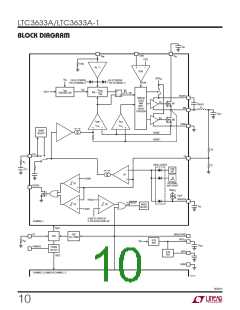
OPERATION
When running the LTC3633A channels out of phase, the
large current pulses are interleaved, effectively reducing
the amount of time the pulses overlap. Thus, the total
RMS input current is decreased, which both relaxes the
One potential disadvantage to this configuration occurs
when one channel is operating at 50% duty cycle. In this
situation, switching noise can potentially couple from one
channel to the other, resulting in frequency jitter on one
or both channels. This effect can be mitigated with a well
designed board layout.
capacitance requirements for the V bypass capacitors
IN
and reduces the voltage noise on the supply line.
APPLICATIONS INFORMATION
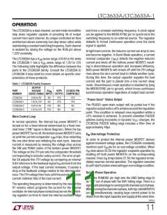
6000
A general LTC3633A application circuit is shown on the
first page of this data sheet. External component selection
is largely driven by the load requirement and switching
frequency. Component selection typically begins with
5000
4000
3000
2000
1000
the selection of the inductor L and resistor R . Once the
T
inductor is chosen, the input capacitor, C , and the out-
IN
put capacitor, C , can be selected. Next, the feedback
OUT
resistors are selected to set the desired output voltage.
Finally,theremainingoptionalexternalcomponentscanbe
selectedforfunctionssuchasexternalloopcompensation,
tracking/soft-start, input UVLO, and PGOOD.
0
0
100 200 300 400 500 600 700
R RESISTOR (kΩ)
T
3633a F01
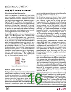
Programming Switching Frequency
Selectionoftheswitchingfrequencyisatrade-offbetween
efficiency and component size. High frequency operation
allows the use of smaller inductor and capacitor values.
Operation at lower frequencies improves efficiency by
reducing internal gate charge losses but requires larger
inductance values and/or capacitance to maintain low
output ripple voltage.
Figure 1. Switching Frequency vs RT
Inductor Selection
Foragiveninputandoutputvoltage,theinductorvalueand
operatingfrequencydeterminetheinductorripplecurrent.
More specifically, the inductor ripple current decreases
with higher inductor value or higher operating frequency
according to the following equation:
Connecting a resistor from the RT pin to SGND programs
the switching frequency (f) between 500kHz and 4MHz
according to the following formula:
⎛
⎞
⎛
⎜
⎝
⎞
⎟
⎠
VOUT
f •L
VOUT
V
IN
ΔI =
1–
⎜
⎟
L
3.2E11
⎝
⎠
RRT
=
f
WhereΔI =inductorripplecurrent,f=operatingfrequency
L
where R is in Ω and f is in Hz.
RT
and L = inductor value. A trade-off between component
size, efficiency and operating frequency can be seen from
When RT is tied to INTV , the switching frequency will
CC
this equation. Accepting larger values of ΔI allows the
default to approximately 2MHz, as set by an internal re-
sistor. This internal resistor is more sensitive to process
and temperature variations than an external resistor
(seeTypicalPerformanceCharacteristics)andisbestused
for applications where switching frequency accuracy is
not critical.
L
useoflowervalueinductorsbutresultsingreaterinductor
core loss, greater ESR loss in the output capacitor, and
larger output voltage ripple. Generally, highest efficiency
operation is obtained at low operating frequency with
small ripple current.
3633a1f
12

 Linear [ Linear ]