LTC3633A/LTC3633A-1
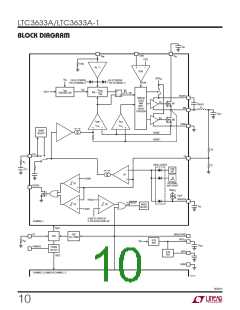
OPERATION
TheLTC3633Aisadual-channel, currentmodemonolithic
step down regulator capable of providing 3A of output
current from each channel. Its unique controlled on-time
architecture allows extremely low step-down ratios while
maintainingaconstantswitchingfrequency. Eachchannel
is enabled by raising the voltage on the RUN pin above
1.22V nominally.
and force a constant switching frequency. A clock signal
can be applied to the MODE/SYNC pin to synchronize the
switching frequency to an external source. The regulator
defaults to forced continuous operation once the clock
signal is applied.
At light load currents, the inductor current can drop to zero
and become negative. In Burst Mode operation, a current
reversal comparator (I ) detects the negative inductor
The LTC3633A has a V sense range of 0.6V to 6V, while
the LTC3633A-1 has a V sense range of 1.5V to 12V.
The following table highlights the difference between the
parts in the LTC3633A family. Consult the LTC3633A-2/
LTC3633A-3 data sheet for more details on specific char-
acteristics of those products.
REV
ON
current and shuts off the bottom power MOSFET, result-
ing in discontinuous operation and increased efficiency.
Both power MOSFETs will remain off until the ITH voltage
rises above the zero current level to initiate another cycle.
During this time, the output capacitor supplies the load
current and the part is placed into a low current sleep
mode. Discontinuous mode operation is disabled by tying
the MODE/SYNC pin to ground, which forces continuous
synchronous operation regardless of output load current.
ON
Table 1. LTC3633A Family Features
OUTPUT
PART
NUMBER
VOLTAGE
SVIN
V2P5
LTC3633 PIN
SENSE RANGE INPUT OUTPUT COMPATIBLE
LTC3633A
0.6V to 6V
1.5V to 12V
0.6V to 6V
1.5V to 12V
NO
NO
YES
YES
NO
YES
YES
NO
“Power Good” Status Output
LTC3633A-1
LTC3633A-2
LTC3633A-3
The PGOOD open-drain output will be pulled low if the
regulatoroutputexitsa 8%windowaroundtheregulation
point. This condition is released once regulation within a
5% window is achieved. To prevent unwanted PGOOD
glitches during transients or dynamic V
LTC3633A PGOOD falling edge includes a filter time of
approximately 40μs.
YES
YES
NO
NO
Main Control Loop
changes, the
OUT
In normal operation, the internal top power MOSFET is
turned on for a fixed interval determined by a fixed one-
shot timer (“ON” signal in Block Diagram). When the top
powerMOSFETturnsoff,thebottompowerMOSFETturns
V Overvoltage Protection
IN
on until the current comparator I
trips, thus restarting
CMP
In order to protect the internal power MOSFET devices
against transient voltage spikes, the LTC3633A constantly
the one shot timer and initiating the next cycle. Inductor
current is measured by sensing the voltage drop across
the SW and PGND nodes of the bottom power MOSFET.
The voltage on the ITH pin sets the comparator threshold
corresponding to inductor valley current. The error ampli-
fier EA adjusts this ITH voltage by comparing an internal
monitors each V pin for an overvoltage condition. When
IN
V rises above 22.5V, the regulator suspends operation by
IN
shutting off both power MOSFETs on the corresponding
channel. Once V drops below 21.5V, the regulator imme-
IN
diately resumes normal operation. The regulator executes
itssoft-startfunctionwhenexitinganovervoltagecondition.
0.6V reference to the feedback signal V derived from the
FB
output voltage. If the load current increases, it causes a
drop in the feedback voltage relative to the internal refer-
ence. The ITH voltage then rises until the average inductor
current matches that of the load current.
Out-Of-Phase Operation
Tying the PHMODE pin high sets the SW2 falling edge to
be 180° out of phase with the SW1 falling edge. There is a
significantadvantagetorunningbothchannelsoutofphase.
Whenrunningthechannelsinphase,bothtop-sideMOSFETs
are on simultaneously, causing large current pulses to be
drawn from the input capacitor and supply at the same time.
3633a1f
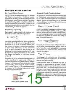
The operating frequency is determined by the value of the
RT resistor, which programs the current for the internal
oscillator.Aninternalphase-lockedloopservostheswitch-
ing regulator on-time to track the internal oscillator edge
11

 Linear [ Linear ]