LTC3407
U
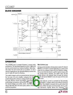
OPERATIO
decrease causes the error amplifier to increase the ITH For lower ripple noise at low currents, the pulse skipping
voltageuntiltheaverageinductorcurrentmatchesthenew mode can be used. In this mode, the LTC3407 continues
load current.
to switch at a constant frequency down to very low
currents, where it will begin skipping pulses.
The main control loop is shut down by pulling the RUN pin
to ground.
Dropout Operation
Low Current Operation
When the input supply voltage decreases toward the
output voltage, the duty cycle increases to 100% which is
the dropout condition. In dropout, the PMOS switch is
turned on continuously with the output voltage being
equal to the input voltage minus the voltage drops across
the internal p-channel MOSFET and the inductor.
Two modes are available to control the operation of the
LTC3407atlowcurrents.Bothmodesautomaticallyswitch
from continuous operation to to the selected mode when
the load current is low.
To optimize efficiency, the Burst Mode operation can be
selected. When the load is relatively light, the LTC3407
automaticallyswitchesintoBurstModeoperationinwhich
the PMOS switch operates intermittently based on load
demand with a fixed peak inductor current. By running
cycles periodically, the switching losses which are domi-
natedbythegatechargelossesofthepowerMOSFETsare
minimized. The main control loop is interrupted when the
output voltage reaches the desired regulated value. A
hysteretic voltage comparator trips when ITH is below
0.35V, shuttingofftheswitchandreducingthepower. The
output capacitor and the inductor supply the power to the
load until ITH exceeds 0.65V, turning on the switch and the
main control loop which starts another cycle.
An important design consideration is that the RDS(ON) of
the P-channel switch increases with decreasing input
supplyvoltage(SeeTypicalPerformanceCharacteristics).
Therefore, the user should calculate the power dissipation
when the LTC3407 is used at 100% duty cycle with low
input voltage (See Thermal Considerations in the Applica-
tions Information Section).
Low Supply Operation
The LTC3407 incorporates an Under-Voltage Lockout
circuit which shuts down the part when the input voltage
drops below about 1.65V to prevent unstable operation.
W U U
U
APPLICATIO S I FOR ATIO
greater core losses, and lower output current capability.
A reasonable starting point for setting ripple current is
∆IL = 0.3 • ILIM, where ILIM is the peak switch current limit.
The largest ripple current ∆IL occurs at the maximum
input voltage. To guarantee that the ripple current stays
below a specified maximum, the inductor value should be
chosen according to the following equation:
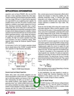
A general LTC3407 application circuit is shown in
Figure 2. External component selection is driven by the
load requirement, and begins with the selection of the
inductor L. Once the inductor is chosen, CIN and COUT can
be selected.
Inductor Selection
Although the inductor does not influence the operating
frequency, the inductor value has a direct effect on ripple
current. The inductor ripple current ∆IL decreases with
⎛
⎞
VOUT
VOUT
L =
• 1–
⎜
⎟
fO • ∆IL
V
IN(MAX)
⎝
⎠
higher inductance and increases with higher VIN or VOUT
:
The inductor value will also have an effect on Burst Mode
operation. The transition from low current operation be-
gins when the peak inductor current falls below a level set
by the burst clamp. Lower inductor values result in higher
VOUT
⎛
VOUT
V
IN
⎞
∆IL =
• 1–
⎜
⎟
fO •L ⎝
⎠
Accepting larger values of ∆IL allows the use of low
inductances, but results in higher output voltage ripple,
ripple current which causes this to occur at lower load
sn3407 3407fs
7

 Linear [ Linear ]