LTC3407
ELECTRICAL CHARACTERISTICS
The ● denotes the specifications which apply over the full operating
temperature range, otherwise specifications are at TA = 25°C. VIN = 3.6V, unless otherwise specified. (Note 2)
SYMBOL
PARAMETER
CONDITIONS
MIN
TYP
MAX
UNITS
POR
Power-On Reset Threshold
V
V
Ramping Up, MODE/SYNC = 0V
Ramping Down, MODE/SYNC = 0V
8.5
–8.5
%
%
FBX
FBX
Power-On Reset On-Resistance
Power-On Reset Delay
RUN Threshold
100
262,144
1
200
Ω
Cycles
V
V
●
●
0.3
1.5
1
RUN
I
RUN Leakage Current
0.01
µA
RUN
Note 1: Absolute Maximum Ratings are those values beyond which the life
V
to the output of the error amplifier.
FB
of a device may be impaired.
Note 4: Dynamic supply current is higher due to the internal gate charge
Note 2: The LTC3407E is guaranteed to meet specified performance from
0°C to 70°C. Specifications over the –40°C and 85°C operating
temperature range are assured by design, characterization and correlation
with statistical process controls.
being delivered at the switching frequency.
Note 5: T is calculated from the ambient T and power dissipation P
D
J
A
according to the following formula: T = T + (P • θ ).
J
A
D
JA
Note 6: The DFN switch on-resistance is guaranteed by correlation to
wafer level measurements.
Note 3: The LTC3407 is tested in a proprietary test mode that connects
U W
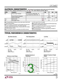
TYPICAL PERFOR A CE CHARACTERISTICS
Load Step
Burst Mode Operation
Pulse Skipping Mode
SW
5V/DIV
SW
5V/DIV
V
OUT
200mV/DIV
V
V
I
L
OUT
100mV/DIV
OUT
10mV/DIV
500mA/DIV
I
L
I
I
LOAD
500mA/DIV
L
200mA/DIV
200mA/DIV
3407 G01
3407 G02
3407 G03
V
V
LOAD
= 3.6V
V
V
LOAD
= 3.6V
V
= 3.6V
IN
4µs/DIV
1µs/DIV
20µs/DIV
IN
IN
= 1.8V
= 1.8V
V
= 1.8V
OUT
OUT
OUT
I
= 50mA
I
= 50mA
I
LOAD
CIRCUIT OF FIGURE 1
= 50mA TO 600mA
CIRCUIT OF FIGURE 1
CIRCUIT OF FIGURE 1
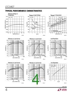
Oscillator Frequency vs Supply
Voltage
Oscillator Frequency vs
Temperature
Efficiency vs Input Voltage
100
95
90
85
80
75
70
65
60
1.70
1.65
1.60
1.55
1.50
1.45
1.40
1.35
1.30
1.8
1.7
1.6
1.5
1.4
1.3
1.2
T
= 25°C
A
T
= 25°C
A
100mA
10mA
1mA
600mA
V
= 1.8V
OUT
CIRCUIT OF FIGURE 1
4
5
6
50
TEMPERATURE (°C)
100 125
4
5
6
2
3
–50 –25
0
25
75
2
3
INPUT VOLTAGE (V)
SUPPLY VOLTAGE (V)
3407 G04
3407 G05
3407 G06
sn3407 3407fs
3

 Linear [ Linear ]