LTC3407
W
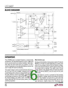
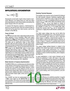
BLOCK DIAGRA
REGULATOR 1
MODE/SYNC
6
BURST
CLAMP
V
IN
SLOPE
COMP
EN
–
+
+
–
0.6V
SLEEP
–
+
I
TH
5Ω
EA
I
COMP
0.35V
V
FB1
1
BURST
Q
S
R
RS
LATCH
Q
0.55V
–
+
SWITCHING
LOGIC
UV
OV
UVDET
OVDET
AND
BLANKING
CIRCUIT
ANTI
SHOOT-
THRU
4
SW1
+
–
0.65V
+
–
I
RCMP
SHUTDOWN
11 GND
V
IN
3
8
V
IN
PGOOD1
POR
2
9
RUN1
RUN2
POR
COUNTER
0.6V REF
OSC
OSC
5
7
GND
PGOOD2
REGULATOR 2 (IDENTICAL TO REGULATOR 1)
10
SW2
V
FB2
U
OPERATIO
Main Control Loop
The LTC3407 uses a constant frequency, current mode
architecture. Theoperatingfrequencyissetat1.5MHzand
can be synchronized to an external oscillator. Both chan-
nels share the same clock and run in-phase. To suit a
variety of applications, the selectable Mode pin allows the
user to trade-off noise for efficiency.
Duringnormaloperation,thetoppowerswitch(P-channel
MOSFET) is turned on at the beginning of a clock cycle
when the VFB voltage is below the the reference voltage.
The current into the inductor and the load increases until
the current limit is reached. The switch turns off and
energy stored in the inductor flows through the bottom
switch (N-channel MOSFET) into the load until the next
clock cycle.
The output voltage is set by an external divider returned to
the VFB pins. An error amplfier compares the divided
outputvoltagewithareferencevoltageof0.6Vandadjusts
the peak inductor current accordingly. Overvoltage and
undervoltage comparators will pull the POR output low if
the output voltage is not within ±8.5%. The POR output
will go high after 262,144 clock cycles (about 175ms) of
achieving regulation.
The peak inductor current is controlled by the internally
compensated ITH voltage, which is the output of the error
amplifier.This amplifier compares the VFB pin to the 0.6V
reference. When the load current increases, the VFB volt-
age decreases slightly below the reference. This
sn3407 3407fs
6

 Linear [ Linear ]