LTC3407
U
U
U
PI FU CTIO S
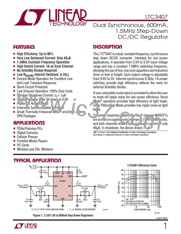
VFB1 (Pin 1): Output Feedback. Receives the feedback
voltage from the external resistive divider across the
output. Nominal voltage for this pin is 0.6V.
be syncronized to an external oscillator applied to this pin
and pulse skipping mode is automatically selected.
SW2 (Pin 7): Regulator 2 Switch Node Connection to the
Inductor. This pin swings from VIN to GND.
RUN1 (Pin 2): Regulator 1 Enable. Forcing this pin to VIN
enables regulator 1, while forcing it to GND causes regu-
lator 1 to shut down.
POR (Pin 8): Power-On Reset . This common-drain logic
output is pulled to GND when the output voltage is not
within ±8.5% of regulation and goes high after 175ms
when both channels are within regulation.
VIN (Pin3):MainPowerSupply.Mustbecloselydecoupled
to GND.
SW1 (Pin 4): Regulator 1 Switch Node Connection to the
RUN2 (Pin 9): Output Feedback. Forcing this pin to VIN
enables regulator 2, while forcing it to GND causes regu-
lator 2 to shut down.
Inductor. This pin swings from VIN to GND.
GND (Pin 5): Main Ground. Connect to the (–) terminal of
COUT, and (–) terminal of CIN.
VFB2 (Pin 10): Output Feedback. Receives the feedback
voltage from the external resistive divider across the
output. Nominal voltage for this pin is 0.6V.
MODE/SYNC (Pin 6): Combination Mode Selection and
OscillatorSynchronization.Thispincontrolstheoperation
of the device. When tied to VIN or GND, Burst Mode
operation or pulse skipping mode is selected, respec-
tively. Do not float this pin. The oscillation frequency can
Exposed Pad (GND) (Pin 11): Power Ground. Connect to
the (–) terminal of COUT, and (–) terminal of CIN. Must be
soldered to electrical ground on PCB.
sn3407 3407fs
5

 Linear [ Linear ]