LTC3101
PIN FUNCTIONS
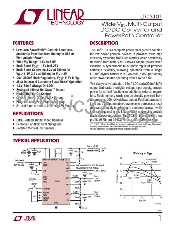
ENA3 (Pin 19): Enable Pin for Buck-Boost Converter.
Forcing this pin above 1V will turn on the buck-boost
converter when the IC is enabled (via the pushbutton
interface). Forcing this pin below 0.3V will disable the
buck-boost converter.
RESET (Pin 13): Active-Low μP Reset and Fault Signal.
This pin provides an active-low microprocessor reset
signal. During the power-up sequence, the μP reset sig-
nal is held low until all converters are in regulation for a
duration programmed by the C capacitor. In addition,
RS
this pin is held low during a fault condition and when the
IC is disabled in order to prevent spurious turn-on of the
microprocessor.
SW3B (Pin 20): Buck-Boost Switch Pin. This pin should
be connected to one side of the buck-boost inductor.
ENA1 (Pin 21): Enable Pin for Buck Converter 1. Forcing
this pin above 1V will turn on the buck converter when the
IC is enabled (via the pushbutton interface). Forcing this
pin below 0.3V will disable buck converter 1.
BAT2 (Pin 14): Battery Power Input for the Buck-Boost
Converter.A10ꢀForlargerbypasscapacitorshouldbecon-
nectedbetweenthispinandground. Thebypasscapacitor
shouldbelocatedasclosetotheICaspossibleandshould
viadirectlydowntothegroundplane. PinsBAT1andBAT2
must be connected together in the application.
FB2(Pin22):FeedbackVoltageInputforBuckConverter 2.
The resistor divider connected to this pin sets the output
voltage for buck converter 2.
SW3A (Pin 15): Buck-Boost Switch Pin. This pin should
be connected to one side of the buck-boost inductor.
FB1(Pin23):FeedbackVoltageInputforBuckConverter 1.
The resistor divider connected to this pin sets the output
voltage for buck converter 1.
USB2 (Pin 16): USB or Wall Adapter Power Input for the
Buck-Boost Converter. A 10ꢀF or larger bypass capacitor
should be connectedfromthispinto ground. Thebypass
capacitor should be located as close to the IC as pos-
sible and should via directly down to the ground plane.
Pins USB1 and USB2 must be connected together in
the application.
ENA2 (Pin 24): Enable Pin for Buck Converter 2. Forcing
this pin above 1V will turn on the buck converter when the
IC is enabled (via the pushbutton interface). Forcing this
pin below 0.3V will disable buck converter 2.
Exposed Pad (Pin 25): Small-Signal and Power Ground
for the IC. The Exposed Pad must be soldered to the PCB
andelectricallyconnectedtogroundthroughtheshortest
and lowest impedance connection possible.
OUT3 (Pin 17): Buck-Boost Output Voltage. This pin is the
power output for the buck-boost regulator. It should be
connected to a low ESR capacitor with a value of at least
10ꢀF. For higher output current applications (>400mA), it
is recommended that a 22μF or larger output capacitor be
used. The capacitor should be placed as close to the IC as
possible and should have a short return path to ground.
HSO(Pin18):HotSwapOutput.Aninternalcurrent-limited
switch connects the HSO output to the buck-boost output
voltage after the buck-boost output reaches regulation.
With the buck-boost operating in PWM mode, this output
is guaranteed to support a 100mA load and is short-circuit
protected.
3101f
11

 Linear [ Linear ]