LTC1698
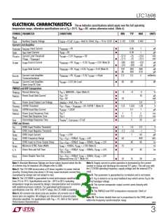
ELECTRICAL CHARACTERISTICS
The ● indicates specifications which apply over the full operating
temperature range, otherwise specifications are at TA = 25°C. VDD = 8V, unless otherwise noted. (Note 4)
SYMBOL PARAMETER
CONDITIONS
MIN
TYP
MAX
UNITS
V
AUX
V
Auxiliary Supply Voltage
C
= 0.1µF, I
= 0mA to 10mA, V = 7V to 12.6V
●
3.135
3.320
3.465
V
AUX
VAUX
LOAD
DD
Current Limit Amplifier
I
I
I
Input Current
V
V
V
= 0V
●
●
0.05
0.05
1
1
µA
µA
ISNSGND SNSGND
ISNSGND
I
Input Current
= 0V
ISNS
ISNS
SNS
V
Current Limit Threshold
(V
= 2.5V, V = 0V
ISNSGND
–27.0
–27.5
–25
–25
–23.0
–22.5
mV
mV
ILIMTH
ICOMP
– V
)
●
●
ISNS
ISNSGND
I
I
Source Current
V
V
V
V
= 0V, V
= 0V, V
= 0V, V
= –0.3V, V = 2.5V (Note 8)
ICOMP
–280
–370
–200
–200
–120
–80
µA
µA
ICOMP
COMP
ISNSGND
ISNSGND
ISNSGND
ISNS
I
Sink Current
= 0.3V, V = 2.5V (Note 8)
ICOMP
120
80
200
200
280
370
µA
µA
COMP
ISNS
●
●
g
Current Limit Amplifier
Transconductance
= 2.5V, I = ±10µA
ICOMP
2.2
3.5
5
millimho
mILIM
ICOMP
G
Current Limit Amplifier
Open-Loop DC Gain
= 2.5V, No Load
ICOMP
●
●
48
60
dB
ICOMP
PWRGD and OVP Comparators
V
Percent Below V
V
↓, MARGIN = Open (Note 9)
–9
10
–6
–3
10
%
PWRGD
PWRGD
FB
FB
I
Power Good Sink Current
V
V
= 2V
= 0V
●
●
µA
mA
FB
FB
V
V
Power Good Output Low Voltage
OVPIN Threshold
I
= 3mA, V = 0V
●
●
●
0.4
1.28
1
V
V
OL
PWRGD
FB
V
V
= V
= V = 0V, OVPIN ↑ (Note 9)
ISNSGND
1.18
1.233
0.1
OVPREF
OVPIN
PWRGD
FB
ISNS
I
t
OVPIN Input Bias Current
= 1.233V
µA
OVPIN
Power Good Response Time
Power Bad Response Time
V
V
↑
↓
●
●
1
0.5
2
1
5
2.5
ms
ms
FB
FB
t
Overvoltage Response Time
V
↑, C = 0.1µF
OPTODRV
●
5
20
µs
OVP
OVPIN
SYNC and Drivers
V
V
SYNC Input Positive Threshold
SYNC Input Negative Threshold
SYNC Input Current
●
●
●
●
●
●
●
1
1.6
–1.6
1
2.2
–1
V
V
PT
–2.2
NT
I
f
t
t
V
C
C
= ±10V
50
µA
kHz
ns
SYNC
SYNC
d
SYNC
SYNC Frequency Range
= C = 1000pF, V
= ±5V
50
75
400
90
FG
CG
SYNC
SYNC Input to Driver Output Delay
Minimum SYNC Pulse Width
Driver Rise and Fall Time
= C = 1000pF, f
= 100kHz, V = ±5V
SYNC
40
10
FG
CG
SYNC
f
= 100kHz, V = ±10V (Note 6)
SYNC
ns
SYNC
SYNC
t , t
r
C
= C = 1000pF, f
= 100kHz, V
= ±5V,
= ±5V
40
ns
f
FG
CG
SYNC
SYNC
10% to 90%
C = C = 1000pF, f
FG
t
Driver Disable Time-Out
= 100kHz, V
DDIS
CG
SYNC
SYNC
Measured from CG ↑ (Note 10)
●
10
15
20
µs
Note 1: Absolute Maximum Ratings are those values beyond which the life
Note 5: Supply current in active operation is dominated by the current
needed to charge and discharge the external FET gates. This will vary with
the LTC1698 operating frequency, supply voltage and the external FETs
used.
of a device may be impaired. All voltages refer to GND.
Note 2: The LTC1698 incorporates a 5V linear regulator to power internal
circuitry. Driving these pins above 5.3V may cause excessive current flow.
Guaranteed by design and not subject to test.
Note 6: This parameter is guaranteed by correlation and is not tested.
Note 3: The LTC1698E is guaranteed to meet performance specifications
from 0°C to 70°C. Specifications over the –40°C to 85°C operating
temperature range are assured by design, characterization and correlation
with statistical process controls. For guaranteed performance to
specifications over the –40°C to 85°C range, the LTC1698I is available.
Note 7: V is tested in an op amp feedback loop which servos V to the
FB
FB
internal bandgap voltage.
Note 8: The current comparator output current varies linearly with
temperature.
Note 9: The PWRGD and OVP comparators incorporate 10mV of
hysteresis.
Note 4: All currents into device pins are positive; all currents out of the
device pins are negative. All voltages are referenced to ground unless
Note 10: The driver disable time-out is proportional to the SYNC period
otherwise specified. For applications with V < 7V, refer to the Typical
DD
within the frequency synchronization range.
Performance Characteristics.
1698f
3

 Linear [ Linear ]