LTC1559-3.3/LTC1559-5
U
W U U
APPLICATIONS INFORMATION
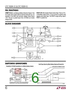
SYSTEM
V
CC
V
CC
LTC1559
+
C
OUT
SYSTEM
REGULATOR
V
BAK
BOOST
CONVERTER
R1
R2
BACKUP
LOGIC
BACKUP
V
REF
PS
1559 F01
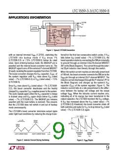
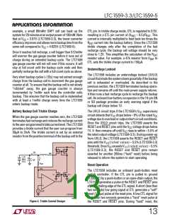
Figure 1. Typical LTC1559 Connection
with an internal trimmed VREF (1.272V), switching the
LTC1559 into backup mode if VCC drops 7%
(LTC1559-3.3) or 7.5% (LTC1559-5) below its rated
value. Upon entering backup mode, the BACKUP pin is
asserted and the internal boost converter turns on. The
BACKUP signal turns off the external P-channel MOSFET
(ifused),isolatingthesystemregulatorfromtheLTC1559.
The boost converter charges the VCC capacitor, COUT, of
the system regulator until VCC rises above VCC (rated
value) – 7% (LTC1559-3.3) or VCC (rated value) – 7.5%
(LTC1559-5).
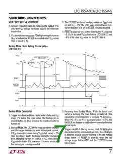
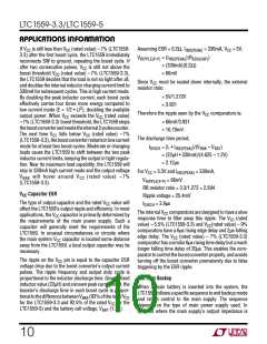
ferred for the first two consecutive switch cycles. If VCC
falls below VCC (rated value) –7% (LTC1559-3.3), the
boost operation starts by connecting the SW pin internally
to ground through an internal 0.5Ω N-channel MOSFET
(N1 in the Block Diagram). The current through the exter-
nal 22µH inductor rises linearly through this switch.
When the switch current reaches an internally preset level
of 165mA, the boost converter connects the SW pin to the
VBAK pin through an internal 2Ω P-channel MOSFET. The
inductor current discharges through the P-channel (P1 in
the Block Diagram) and charges up the system’s VCC
capacitor (COUT of the system regulator, Figure 1). The
inductor current falls at a rate proportional to the differ-
ence between the backup cell voltage and the output
voltage VBAK. When the inductor current reaches zero,
indicating all of its energy has been transferred to the
output capacitor, the LTC1559 monitors the VCC voltage.
If VCC has increased above the VCC (rated value) –7%
(LTC1559-3.3) threshold, the boost converter shuts off
both switches and waits for VCC to drop below VCC (rated
value) –7% (LTC1559-3.3) again.
Once VCC rises above VCC (rated value) – 7% (LTC1559-
3.3), the boost converter deactivates and the freshly
chargedVCC capacitorCOUT suppliespowertothesystem.
The cycle repeats again when the VCC capacitor’s charge
is drained away and VCC again drops below VCC (rated
value) – 7% (LTC1559-3.3). The BACKUP pin remains
asserted until the main battery is restored. This ensures
that the LTC1559 does not switch in and out of backup
mode unnecessarily.
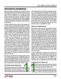
The LTC1559’s boost converter minimizes output ripple
under light load conditions by reducing the charge trans-
1
BOOST
CYCLE
330mA
(PEAK)
V
BAK
ESR RIPPLE
165mA
(PEAK)
1559 F03
DISCHARGE
PERIOD
CHARGE
PERIOD
CH
1559 F02
LIGHT CURRENT MODE
HEAVY CURRENT MODE
t
t
DISCH
Figure 2. Inductor Current During Switching
Figure 3. VBAK Ripple
9

 Linear [ Linear ]