LTC1559-3.3/LTC1559-5
U
W U U
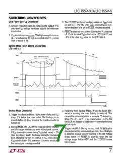
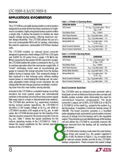
APPLICATIONS INFORMATION
high when inactive (typically a boost regulator with an
output catch diode), the LTC1559 detects the return of the
main supply by watching for VCC to exceed VCC (rated
value) – 5.5% (LTC1559-3.3). The LTC1559 then shuts
down its internal boost converter and begins to recharge
the NiCd cell. In such applications, the PS pin is not used
and can be tied to ground. No external P-channel MOSFET
is required to isolate the main supply from the system VCC
during backup.
to the load while charge on the VCC capacitor drains away.
If VCC drops below VCC (rated voltage) –9% for more than
7.5µs, the LTC1559’s VCC supervisory circuit activates
UVLO mode, shutting off the boost converter and assert-
ing the Reset pins. The 7.5µs delay prevents the LTC1559
from being fooled by brief transients or noise spikes on its
V
CC pin. Upon receipt of the reset signal, the host system
should shut down in an orderly manner. The LTC1559’s
V
CC supervisory circuit will remain alive until VCC is less
than 1V to ensure a valid RESET pin signal.
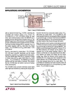
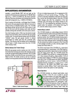
In systems where the main supply’s output impedance is
low when inactive (typically buck regulators), the main
supply must be disconnected from the system VCC during
backup to prevent the inactive supply from loading the
LTC1559. This is typically accomplished using an external
P-channel MOSFET as shown in Figure 1. When the main
supply is restored, the P-channel MOSFET’s body diode
forward-biases. This allows current to flow into the sys-
tem VCC, but the forward drop across this diode may
prevent VCC from reaching the VCC (rated value)
– 5.5% (LTC1559-3.3) threshold that deactivates the
LTC1559’s backup mode. In such systems, the PS pin
should connect directly to the output of the main system
supply. When the system regulator’s voltage rises about
2.5% above the backup VCC, the PS comparator triggers
and causes the LTC1559 to deassert the BACKUP pin
signal. This signals the system controller to restore sys-
tem loading and resume normal operation. At the same
time, the external P-MOSFET is driven by the BACKUP
signal. The P-channel MOSFET turns on and allows the
main regulator to bypass its body diode and drive the
system VCC directly.
Backup Cell Voltage Monitoring
As the boost converter removes charge from the backup
NiCd cell, the cell’s terminal voltage falls. Permanent
damage to the NiCd cell can occur if it is discharged to
below 0.9V. To prevent this, the LTC1559 monitors the
cell’s terminal voltage through the CTL pin during backup.
If the CTL pin drops below 0.9V for more than 20µs, the
UVLO circuit shuts down the boost converter and asserts
the RESET and RESET pins. Since the CTL pin can also be
connected to an external push-button reset, the LTC1559
includes internal logic to ensure that the low cell voltage
reset is triggered only if the CTL pin is between 0.9V and
0.25V. This will prevent a push-button reset (which pulls
CTL below 250mV) from being mistaken as a low cell
voltage condition. Unusual situations where the NiCd cell
voltage drops drastically below 0.25V will also trigger
UVLO, since the LTC1559 will treat this as a “hard” reset
after two seconds.
AnoptionalLOBAToutput,availableinthe16-pinGNorSO
package, can be used to signal the system if the cell
voltage falls below 1V, giving an early warning that the
backup cell is heavily discharged. The LOBAT pin is
disabled if the LTC1559 is in trickle charge mode,
because the CTL pin is regulated to 0.5V by the LTC1559.
Sincetheusercanreplacethemainbatteryanytimeduring
the LTC1559’s backup operation, the BACKUP signal may
be deasserted while the boost converter is switching. To
prevent the potential problem of residual energy in the
inductor, the LTC1559 will only stop the boost converter
after it completes the current boost converter cycle.
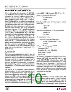
Fault Protection and Thermal Limit
The LTC1559’s boost converter incorporates two internal
timers that turn off the switch transistors if the inductor
charge or discharge time gets abnormally long.
UVLO Under Excessive Backup Load
Very heavy loads (above the LTC1559’s maximum power
output) will pull the boost converter’s output below the
boost threshold. Under these conditions, the LTC1559’s
boostconvertercontinuestosupply330mAcurrentpulses
The inductor charge time may get abnormally long if the
NiCdcellvoltagedropsbelow0.25Vwithouttriggeringthe
0.25V < VBAT < 0.9V low cell voltage comparator. In this
11

 Linear [ Linear ]