LTC1559-3.3/LTC1559-5
U
U
U
PIN FUNCTIONS
Pin Numbers Are Shown First for the SO-8 Package
Then the GN16 and S16 Packages
is guaranteed to be valid when VCC is greater than or equal
to 1V.
SW (Pins 1/1, 2): Boost Converter Switching Node. Con-
nect a 22µH inductor from SW to the positive terminal of
the backup cell. In backup mode, this node is alternately
switchedbetweengroundandVBAK,generatingthebackup
output voltage. In fast or trickle charge mode, an internal
regulator outputs a constant DC current from this pin
through the 22µH inductor and into the NiCd battery.
Duringpower-uporundervoltagelockout(UVLO), theSW
pin enters a high impedance state.
RESET also provides a low going 100µs signal whenever
the CTL pin is pulled low for less than two seconds (“soft”
reset). Unlike hard reset, soft reset does not affect the
LTC1559’s current operating mode.
BACKUP (Pins 6/13): System Backup Signal. This is a
TTL-compatible output driver that pulls low unless the
LTC1559 is in backup mode. BACKUP signals the system
controller that the system is in backup mode so that it can
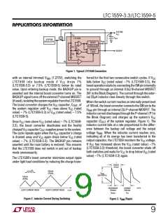
reduce system loading. BACKUP can also be used to drive
the gate of a P-channel MOSFET in series with the main
system regulator’s output. See the Applications Informa-
tion section for more details.
GND (Pins 2/4): System Ground. The low power internal
circuitry returns to this pin in the 16-pin packages. GND
and PGND are bonded together to this pin in the 8-pin
package.
V
CC (Pins 7/14): Power Supply Input. All internal circuits
CTL (Pins 3/5): Control. This pin provides three functions.
In backup mode this pin is a high impedance input and
monitors the backup battery cell voltage (VBAT). If VBAT
drops below 0.9V, the LTC1559 enters UVLO. During
trickle charge mode, an external resistor REXT sets the
trickle charge current. In all modes, pulling the CTL pin
below 250mV generates either a “soft” or “hard” reset
pulse. See the Applications Information section for more
information.
except the boost converter are powered from this pin. A
0.1µF bypass capacitor is required from VCC to ground.
The UVLO detector inside the LTC1559 monitors VCC. If
VCC drops below the rated output voltage by 9%, the
LTC1559 enters UVLO mode and RESET is asserted. The
LTC1559-3.3 exits UVLO if VCC rises to greater than
–5.5% of the rated output voltage. The LTC1559-5 exits
UVLO if VCC rises to greater than –6% of the rated output
voltage.SeetheApplicationsInformationsectionformore
details.
PS (Pins 4/7): Power Supply Sense. This pin senses the
presence of the main supply and triggers the LTC1559 to
terminate backup mode. During backup, VCC is driven
externallybytheLTC1559’sboostconvert’soutput(VBAK).
When PS > VCC during backup, the LTC1559 pulls down
the BACKUP pin, reconnecting the system regulator out-
puttothesystemVCC. ThePSpinisneededinapplications
that use a P-channel MOSFET (driven by the BACKUP
signal) to isolate the system regulator during backup. If
not needed, PS can be disabled by tying it to ground.
VBAK(Pins8/15,16):BackupSupplyOutput.TheLTC1559’s
boost converter provides the regulated output voltage to
the system through VBAK during backup mode.
16-Pin GN and SO Packages
PGND (Pin 3): Power Ground. The internal driver circuitry
returns to this pin. PGND should be connected to a low
impedance ground plane in close proximity to the NiCd
battery cell.
SHDN (Pin 6): Chip Shutdown. A TTL-compatible active
low voltage at SHDN puts the LTC1559 into low power
shutdown mode. In shutdown, all internal circuits power
down and are held in a reset state. The SW, CTL and VBAK
pins enter into high impedance states. In shutdown mode,
supply current drops to below 50µA and current drawn
from the backup cell drops to below 15µA.
RESET (Pins 5/11): System Reset, Active Low. This is an
open-drain output. This pin provides a low going reset
signal to the system processor. A 200ms pulse is gener-
ated if the CTL pin is pulled low for more than two seconds
(“hard” reset) or if the LTC1559 comes out of UVLO. This
“hard reset” stops the internal boost converter if it is
running. This pin is held low if the LTC1559 is in UVLO and
5

 Linear [ Linear ]