LTC1559-3.3/LTC1559-5
W U U
U
APPLICATIONS INFORMATION
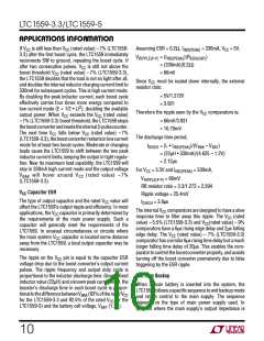
20ms < t
< 2s
CTL
(A)
0V
(B)
shut off completely. Note that the backup cell slowly
discharges through REXT in this mode.
>0.25V
CTL
t
< 20ms
CTL
Inductor Selection
RESET
100µs
100µs
20ms
The LTC1559 is designed to operate with a recommended
inductorvalueof22µH(±20%)with<0.2ΩDCresistance.
DEBOUNCE
“SOFT” PUSH-BUTTON RESET AT CTL
(A) CTL < 0.25V FOR LESS THAN 20ms
(B) CTL > 0.25V FOR MORE THAN 20ms
Usinginductorvaluesabove22µHwilldelivermoreoutput
power but will cause the gas gauge counter to count
inaccurately and under-recharge the backup cell. At the
same time, the N-channel transistor timer will limit the
peak current if the charging time becomes overextended
due to the higher inductor value. Using inductor values
lower than 22µH will degrade the boost converter’s maxi-
mum output power and cause the gas gauge counter to
overcharge the backup cell. Table 3 lists a few recom-
mended surface mount inductor part numbers.
>0.25V
0V
CTL
t
> 2s
CTL
RESET
2s
200ms
“HARD” PUSH-BUTTON RESET AT CTL
CTL < 0.25V FOR MORE THAN 2s
0V
CTL
20ms
RESET
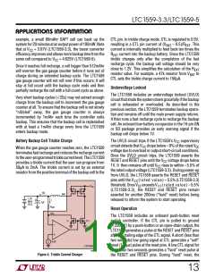
Table 3. Recommended Inductors
20ms
PART
NUMBER
TYP INDUCTOR
VALUE
DCR
(Ω)
1559 F05
20ms DEBOUNCE AT FALLING AND RISING RESET EDGE
MANUFACTURER
Sumida
CD54-220
22µH ±20%
22µH ±20%
0.18
Figure 5. Push-Button Resets
Sumida
CDRH73/74
0.2/0.11
LTC1559 disables the boost converter if it is in backup
mode. All signals at the CTL pin are debounced for 20ms
to prevent multiple resets, allowing the CTL pin to be
connected directly to a push-button to ground.
Capacitor Selection
The LTC1559 requires a VCC capacitor of 100µF to ensure
that boost converter can regulate the output under maxi-
mum load conditions. The capacitor’s ESR should be
small (<0.2Ω) to minimize voltage spikes that might
incorrectly trigger the LTC1559’s internal VCC compara-
tors. Note that the LTC1559 can usually share the output
capacitor with the system regulator. However, a 1µF is
recommended directly at the LTC1559’s VCC pin. The VCC
capacitor’s ratings like VMAX, IRIPPLE(RMS) all must meet
the system regulator’s specifications as well.
The RESET pin is an open-drain output that requires an
external pull-up resistor. The RESET pin is a TTL compat-
ible CMOS output.
Shutdown
The 16-pin LTC1559 has a TTL compatible input, SHDN
that shuts down the whole chip, asserts the RESET and
RESET pins and places the CTL, VBAK and SW pins into
high impedance states. The SHDN pin has an internal pull-
upof8µAthatensuresthechipwillnotshutdownifthepin
is left floating. The chip consumes less than 50µA during
shutdown.
Battery Selection
A primary application for the LTC1559 is a “bridging”
supply, only providing backup current while the main
system battery is being replaced. In these applications,
the LTC1559 works well with NiCd button cells or small
cylindricalcells, reducingsystemcostsandboardspace.
It is optimized for use with up to 512mAhr battery
capacities.
Although there is no SHDN pin for the SO-8 package, the
user can shut down the part by pulling CTL to ground. The
chip enters “hard” reset leaving only the bandgap and
comparators alive. The charger and the boost converter
14

 Linear [ Linear ]