LTC1278
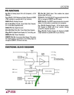
O U
W
U
PPLICATI
A
S I FOR ATIO
INPUT RANGE
conversion starts. Any op amp that settles in 200ns to
small current transients will allow maximum speed opera-
tion. If slower op amps are used, more settling time can be
provided by increasing the time between conversions.
Suitable devices capable of driving the ADC’s AIN input
include the LT1360, LT1220, LT1223 and LT1224 op
amps.
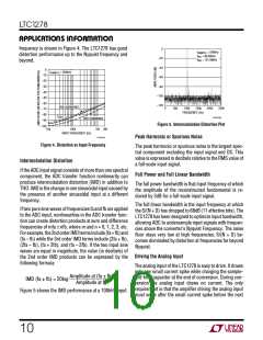
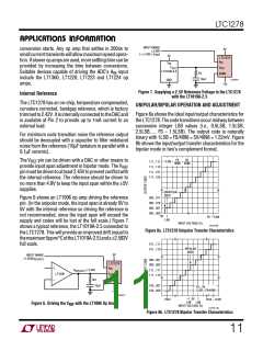
5V
±2.58V
(= ±1.033 × V
)
REF
5V
LTC1278
A
IN
V
IN
V
V
REF
OUT
LT1019A-2.5
3Ω
10µF
AGND
LTC1278 F7
GND
–5V
Figure 7. Supplying a 2.5V Reference Voltage to the LTC1278
with the LT1019A-2.5
Internal Reference
The LTC1278 has an on-chip, temperature compensated,
curvature corrected, bandgap reference, which is factory
trimmedto2.42V. ItisinternallyconnectedtotheDACand
is available at Pin 2 to provide up to 1mA current to an
external load.
UNIPOLAR/BIPOLAR OPERATION AND ADJUSTMENT
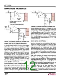
Figure 8a shows the ideal input/output characteristics for
theLTC1278. Thecodetransitionsoccurmidwaybetween
successive integer LSB values (i.e., 0.5LSB, 1.5LSB,
2.5LSB, ... FS – 1.5LSB). The output code is naturally
binary with 1LSB = FS/4096 = 5V/4096 = 1.22mV. Figure
8b shows the input/output transfer characteristics for the
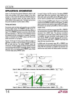
bipolar mode in two’s complement format.
For minimum code transition noise the reference output
should be decoupled with a capacitor to filter wideband
noise from the reference (10µF tantalum in parallel with a
0.1µF ceramic).
FS
5V
The VREF pin can be driven with a DAC or other means to
provide input span adjustment in bipolar mode. The VREF
pinmustbedriventoatleast2.45Vtopreventconflictwith
the internal reference. The reference should be driven to
no more than 4.8V to keep the input span within the ±5V
supplies.
1LSB =
=
111...111
111...110
111...101
111...100
4096 4096
UNIPOLAR
ZERO
000...011
000...010
000...001
000...000
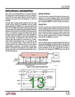
Figure 6 shows an LT1006 op amp driving the reference
pin. (In the unipolar mode, the input span is already 0V to
5V with the internal reference so driving the reference is
not recommended, since the input span will exceed the
supply and codes will be lost at the full scale.) Figure 7
shows a typical reference, the LT1019A-2.5 connected to
the LTC1278. This will provide an improved drift (equal to
themaximum5ppm/°CoftheLT1019A-2.5)anda±2.582V
full scale.
0V
1
LSB
FS – 1LSB
INPUT VOLTAGE (V)
LTC1278 F8a
Figure 8a. LTC1278 Unipolar Transfer Characteristics
011...111
BIPOLAR
ZERO
011...110
5V
INPUT RANGE
±1.033V
REF(OUT)
000...001
000...000
111...111
111...110
LTC1278
A
+
–
IN
V
≥ 2.45V
3Ω
REF(OUT)
LT1006
V
REF
AGND
100...001
100...000
10µF
FS = 5V
1LSB = FS/4096
–5V
LTC1278 F6
–1 0V
1
–FS/2
FS/2 – 1LSB
LSB
LSB
Figure 6. Driving the VREF with the LT1006 Op Amp
INPUT VOLTAGE (V)
LTC1278 • F8b
Figure 8b. LTC1278 Bipolar Transfer Characteristics
11

 Linear [ Linear ]