LTC1278
O U
W
U
PPLICATI
S I FOR ATIO
A
Also, since any potential difference in grounds between
the signal source and ADC appears as an error voltage in
series with the input signal, attention should be paid to
reducing the ground circuit impedances as much as
possible.
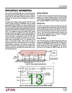
DIGITAL INTERFACE
The A/D converter is designed to interface with micropro-
cessors as a memory mapped device. The CS and RD
controlinputsarecommontoallperipheralmemoryinterfac-
ing. A separate CONVST is used to initiate a conversion.
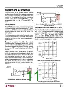
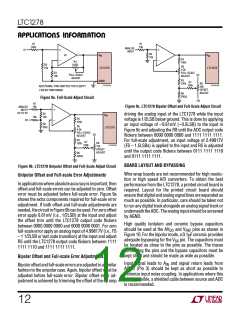
A single point analog ground separate from the logic
system ground should be established with an analog
groundplaneatPin3(AGND)orascloseaspossibletothe
ADC. Pin 12 (DGND) and all other analog grounds should
be connected to this single analog ground point. No other
digitalgroundsshouldbeconnectedtothisanalogground
point. Low impedance analog and digital power supply
common returns are essential to low noise operation of
the ADC and the foil width for these tracks should be as
wide as possible. In applications where the ADC data
outputs and control signals are connected to a continu-
ously active microprocessor bus, it is possible to get
errors in conversion results. These errors are due to
feedthrough from the microprocessor to the successive
approximation comparator. The problem can be elimi-
nated by forcing the microprocessor into a WAIT state
during conversion or by using three-state buffers to iso-
late the ADC data bus.
Internal Clock
The A/D converter has an internal clock that eliminates the
need of synchronization between the external clock and
the CS and RD signals found in other ADCs. The internal
clock is factory trimmed to achieve a typical conversion
time of 1.6µs. No external adjustments are required, and
with the typical acquisition time of 250ns, throughput
performance of 500ksps is assured.
Power Shutdown
The LTC1278 provides a shutdown feature that will save
powerwhentheADCisininactiveperiods. Topowerdown
the ADC, Pin 18 (SHDN) needs to be driven low. When in
power shutdown mode, the LTC1278 will not start a
conversion even though the CONVST goes low. All the
1
DIGITAL
SYSTEM
LTC1278
A
IN
AGND
3
V
AV
DV
DGND
12
REF
2
DD
24
DD
17
+
–
ANALOG
INPUT
CIRCUITRY
GROUND CONNECTION
TO DIGITAL CIRCUITRY
10µF
0.1µF
10µF
0.1µF
ANALOG GROUND PLANE
LTC1278 F10
Figure 10. Power Supply Grounding Practice
ACTIVE HIGH
RD
CS
ENABLE THREE-STATE OUTPUTS
DB11....DB0
BUSY
CONVERSION
START (RISING
EDGE TRIGGER)
D
Q
FLIP
CONVST
SHDN
FLOP
CLEAR
LTC1278 F11
Figure 11. Internal Logic for Control Inputs CS, RD, CONVST and SHDN
13

 Linear [ Linear ]