LTC1278
O U
S
W
U
PPLICATI
I FOR ATIO
A
R1
50Ω
R1
10k
ANALOG
INPUT
V1
+
–
+
–
R2
10k
A1
A
IN
A
IN
R4
100k
R4
100Ω
R2
10k
R5
4.3k
LTC1278
LTC1278
FULL-SCALE
ADJUST
R3
FULL-SCALE
ADJUST
5V
10k
R3
AGND
R7
R8
20k
100k
LTC1278 F9a
LTC1278 F9c
100k
ADDITIONAL PINS OMITTED FOR CLARITY
OFFSET
ADJUST
±20LSB TRIM RANGE
R6
200Ω
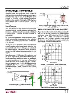
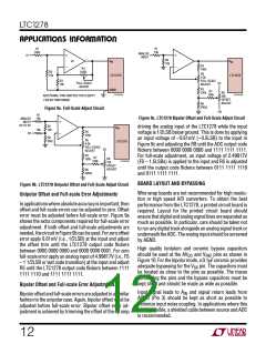
Figure 9a. Full-Scale Adjust Circuit
–5V
R1
10k
Figure 9c. LTC1278 Bipolar Offset and Full-Scale Adjust Circuit
ANALOG
INPUT
+
0V TO 5V
R2
driving the analog input of the LTC1278 while the input
voltage is 1/2LSB below ground. This is done by applying
an input voltage of –0.61mV (–0.5LSB) to the input in
Figure 9c and adjusting the R8 until the ADC output code
flickers between 0000 0000 0000 and 1111 1111 1111.
For full-scale adjustment, an input voltage of 2.49817V
(FS – 1.5LSBs) is applied to the input and R5 is adjusted
until the output code flickers between 0111 1111 1110
and 0111 1111 1111.
A
IN
10k
10k
R4
5V
–
100k
R9
20Ω
R5
4.3k
FULL-SCALE
ADJUST
LTC1278
5V
R3
100k
R7
R8
10k
LTC1278 F9b
100k
OFFSET
ADJUST
R6
400Ω
BOARD LAYOUT AND BYPASSING
Figure 9b. LTC1278 Unipolar Offset and Full-Scale Adjust Circuit
Wire wrap boards are not recommended for high resolu-
tion or high speed A/D converters. To obtain the best
performance from the LTC1278, a printed circuit board is
required. Layout for the printed circuit board should
ensure that digital and analog signal lines are separated as
much as possible. In particular, care should be taken not
to run any digital track alongside an analog signal track or
underneath the ADC. The analog input should be screened
by AGND.
Unipolar Offset and Full-scale Error Adjustments
Inapplicationswhereabsoluteaccuracyisimportant,then
offset and full-scale errors can be adjusted to zero. Offset
error must be adjusted before full-scale error. Figure 9a
shows the extra components required for full-scale error
adjustment. If both offset and full-scale adjustments are
needed, thecircuitinFigure9bcanbeused. Forzerooffset
error apply 0.61mV (i.e., 1/2LSB) at the input and adjust
the offset trim until the LTC1278 output code flickers
between 0000 0000 0000 and 0000 0000 0001. For zero
full-scale error apply an analog input of 4.99817V (i.e., FS
– 1 1/2LSB or last code transition) at the input and adjust
R5 until the LTC1278 output code flickers between 1111
1111 1110 and 1111 1111 1111.
High quality tantalum and ceramic bypass capacitors
should be used at the AVDD and VREF pins as shown in
Figure 10. For the bipolar mode, a 0.1µF ceramic provides
adequate bypassing for the VSS pin. The capacitors must
be located as close to the pins as possible. The traces
connecting the pins and the bypass capacitors must be
kept short and should be made as wide as possible.
Bipolar Offset and Full-scale Error Adjustments
Input signal leads to AIN and signal return leads from
AGND (Pin 3) should be kept as short as possible to
minimize input noise coupling. In applications where this
is not possible, a shielded cable between source and ADC
is recommended.
Bipolaroffsetandfull-scaleerrorsareadjustedinasimilar
fashion to the unipolar case. Again, bipolar offset must be
adjusted before full-scale error. Bipolar offset error ad-
justment is achieved by trimming the offset of the op amp
12

 Linear [ Linear ]