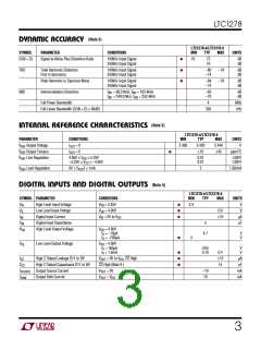
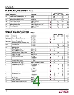
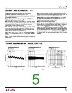
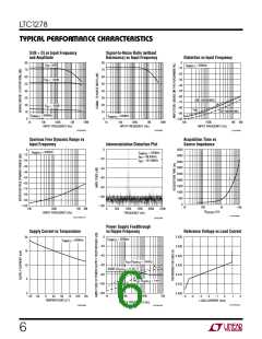
LTC1278
U U
U
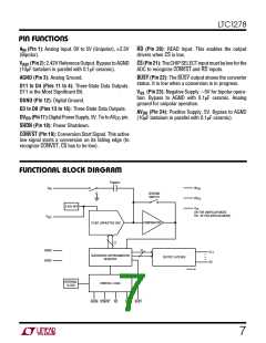
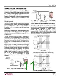
PI FU CTIO S
A (Pin 1): Analog Input. 0V to 5V (Unipolar), ±2.5V RD (Pin 20): READ Input. This enables the output
IN
(Bipolar).
drivers when CS is low.
V
(Pin 2): 2.42V Reference Output. Bypass to AGND CS(Pin21):TheCHIPSELECTinputmustbelowforthe
REF
(10µF tantalum in parallel with 0.1µF ceramic).
ADC to recognize CONVST and RD inputs.
AGND (Pin 3): Analog Ground.
BUSY (Pin 22): The BUSY output shows the converter
status. It is low when a conversion is in progress.
D11 to D4 (Pins 11 to 4): Three-State Data Outputs.
D11 is the Most Significant Bit.
V
(Pin 23): Negative Supply. –5V for bipolar opera-
SS
tion. Bypass to AGND with 0.1µF ceramic. Analog
DGND (Pin 12): Digital Ground.
ground for unipolar operation.
D3 to D0 (Pins 13 to 16): Three-State Data Outputs.
DV (Pin17):Digital Power Supply, 5V. Tie to AV pin.
AV (Pin 24): Positive Supply, 5V. Bypass to AGND
DD
(10µF tantalum in parallel with 0.1µF ceramic).
DD
DD
SHDN (Pin 18): Power Shutdown.
CONVST (Pin 19): Conversion Start Signal. This active
low signal starts a conversion on its falling edge (to
recognize CONVST, CS has to be low).
U
U
W
FU CTIO AL BLOCK DIAGRA
C
SAMPLE
A
AV
DD
IN
ZEROING
SWITCH
DV
DD
2.42V REF
V
SS
(0V FOR UNIPOLAR MODE
OR –5V FOR BIPOLAR MODE)
V
REF
COMPARATOR
12-BIT CAPACITIVE DAC
12
AGND
DGND
12
D11
•
SUCCESSIVE APPROXIMATION
REGISTER
OUTPUT LATCHES
•
•
D0
LTC1278 • BD
INTERNAL
CLOCK
CONTROL LOGIC
SHDN CONVST RD
CS
BUSY
7

 Linear [ Linear ]