LTC1278
PPLICATI
O U
W
U
A
S I FOR ATIO
power is off except the Internal Reference which is still
active and provides 2.42V output voltage to the other
circuitry. In this mode the ADC draws 8.5mW instead of
75mW (for minimum power, the logic inputs must be
within 600mV of the supply rails). The wake-up time from
the power shutdown to active state is 350ns.
In mode 2 (Figure 14) CS is tied low. The falling CONVST
signal again starts the conversion. Data outputs are in
three-state until read by MPU with the RD signal. Mode 2
can be used for operation with a shared MPU databus.
In Slow memory and ROM modes (Figures 15 and 16) CS
istiedlowandCONVSTandRDaretiedtogether. TheMPU
starts conversion and read the output with the RD signal.
Conversions are started by the MPU or DSP (no external
sample clock).
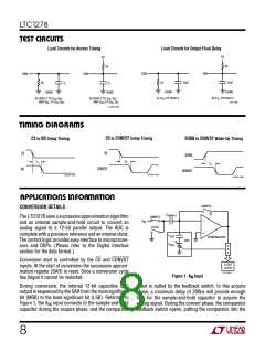
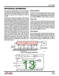
Timing and Control
Conversion start and data read operations are controlled
by three digital inputs: CS, CONVST and RD. Figure 11
shows the logic structure associated with these inputs. A
logic “0” for CONVST will start a conversion after the ADC
has been selected (i.e., CS is low). Once initiated it cannot
be restarted until the conversion is complete. Converter
status is indicated by the BUSY output, and this is low
while conversion is in progress.
InSlowmemorymodetheprocessortakesRD(=CONVST)
low and starts the conversion. BUSY goes low forcing the
processor into a WAIT state. The previous conversion
result appears on the data outputs. When the conversion
is complete, the new conversion results appear on the
data outputs; BUSY goes high releasing the processor,
and the processor takes RD (= CONVST) back high and
reads the new conversion data.
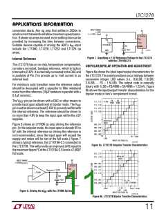
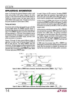
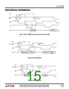
Figures 12 through 16 show several different modes of
operation. In modes 1a and 1b (Figures 12 and 13) CS and
RD are both tied low. The falling CONVST starts the
conversion. The data outputs are always enabled and data
can be latched with the BUSY rising edge. Mode 1a shows
operation with a narrow low going CONVST pulse. Mode
1b shows high going CONVST pulse.
In ROM mode, the processor takes RD (= CONVST) low
which starts a conversion and reads the previous conversion
result. After the conversion is complete, the processor can
read the new result (which will initiate another conversion).
t
CS = RD = 0
CONVST
CONV
t
4
SAMPLE N
SAMPLE N + 1
t
5
BUSY
DATA
t
6
DATA (N-1)
DB11 TO DB0
DATA N
DB11 TO DB0
DATA (N + 1)
DB11 TO DB0
LTC1278 F12
Figure 12. Mode 1a. CONVST Starts a Conversion. Data Ouputs Always Enabled.
(CONVST =
)
t
CS = RD = 0
CONV
t
11
SAMPLE N
SAMPLE N + 1
CONVST
t
5
t
5
BUSY
DATA
t
6
DATA (N-1)
DB11 TO DB0
DATA N
DB11 TO DB0
DATA (N + 1)
DB11 TO DB0
LTC1278 F13
Figure 13. Mode 1b. CONVST Starts a Conversion. Data Outputs Always Enabled.
(CONVST =
)
14

 Linear [ Linear ]