LT8705
APPLICATIONS INFORMATION
rising edge or the SYNC pin’s rising edge if it is toggling.
CLKOUT toggles only in normal mode (see Figure 2).
a reduction of maximum inductor current in the boost
region, and an increase of the maximum inductor current
in the buck region. For example, refer to the Maximum
InductorCurrentSenseVoltagevsDutyCyclegraphinthe
Typical Performance Characteristics section. The graph
showsthat,withVCatitsmaximumvoltage,themaximum
inductor sense voltage VRSENSE is between 78mV and
117mV depending on the duty cycle. It also shows that
the maximum inductor valley current in the buck region
is 86mV increasing to ~130mV at higher duty cycles.
The CLKOUT pin can be used to synchronize other de-
vices to the LT8705’s switching frequency. For example,
the CLKOUT pin can be tied to the SYNC pin of another
LT8705 regulator which will operate approximately 180°
out of phase of the master LT8705 due to the CLKOUT
phase shift. The frequency of the master LT8705 can be
set by the external R resistor or by toggling the SYNC
T
pin. CLKOUTwillbeginoscillatingafterthemasterLT8705
enters normal mode (see Figure 2). Note that the RT pin
of the slave LT8705 must have a resistor tied to ground.
R
SENSE
Selection and Maximum Current
TheR
resistancemustbechosenproperlytoachieve
In general, use the same value R resistor for all of the
SENSE
T
thedesiredamountofoutputcurrent.Toomuchresistance
synchronized LT8705s.
can limit the output current below the application require-
The duty cycle of CLKOUT is proportional to the die tem-
perature and can be used to monitor the die for thermal
issues.SeetheJunctionTemperatureMeasurementsection
for more information.
ments.StartbydeterminingthemaximumallowedR
SENSE
resistanceintheboostregion, R
. Follow
SENSE(MAX,BOOST)
this by finding the maximum allowed R
resistance in
SENSE
the buck region, R
. The selected R
SENSE(MAX,BUCK)
SENSE
resistance must be smaller than both.
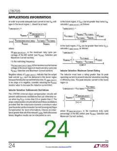
Boost Region: In the boost region, the maximum output
current capability is the least when V is at its minimum
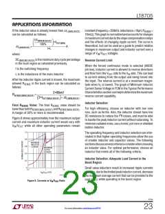
Inductor Current Sensing and Slope Compensation
TheLT8705operatesusinginductorcurrentmodecontrol.
As described previously in the Power Switch Control sec-
tion,theLT8705measuresthepeakoftheinductorcurrent
waveformintheboostregionandthevalleyoftheinductor
current waveform in the buck region. The inductor current
IN
and V
is at its maximum. Therefore R
must be
OUT
SENSE
chosen to meet the output current requirements under
these conditions.
is sensed across the R
resistor with pins CSP and
Start by finding the boost region duty cycle when V is
IN
SENSE
CSN. During any given cycle, the peak (boost region) or
minimum and V
is maximum using:
OUT
valley (buck region) of the inductor current is controlled
V
IN(MIN)
by the V pin voltage.
C
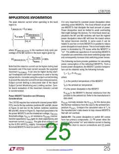
DC(MAX,M3,BOOST) ≅ 1–
•100%
V
OUT(MAX)
Slope compensation provides stability in constant-
frequencycurrentmodecontrolarchitecturesbyprevent-
ing subharmonic oscillations at high duty cycles. This
is accomplished internally by adding a compensating
ramp to the inductor current signal in the boost region,
or subtracting a ramp from the inductor current signal
in the buck region. At higher duty cycles, this results in
For example, an application with a V range of 12V to
IN
48V and V
set to 36V will have:
OUT
12V
36V
DC(MAX,M3,BOOST) ≅ 1–
•100%= 67%
8705p
21
For more information www.linear.com/8705

 Linear [ Linear ]