LT5581
APPLICATIONS INFORMATION
resulting deviation in the output voltage of the detector
shows the effect of the internal 150kHz filter.
It is important that the voltage applied to the EN pin never
exceeds V by more than 0.5V, otherwise, the supply
CC
current may be sourced through the upper ESD protection
diode connected at the EN pin.
The output voltage noise density and integrated noise are
showninFigures12and13, respectively, forvariousinput
powerlevels.Noiseisastrongfunctionofinputlevel.There
is roughly a 10dB reduction in the output noise level for
an input level of 0dBm versus no input.
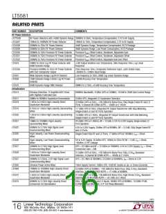
V
LT5581
EN
CC
2
Enable Pin
500k
300k
300k
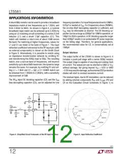
A simplified schematic of the EN pin is shown in Figure
14. To enable the LT5581, it is necessary to put greater
than 1V on this pin. To disable or turn off the chip, this
voltage should be below 0.3V. At an enable voltage of
3.3V, the pin draws roughly 20μA. If the EN pin is not
connected, the chip is disabled through an internal 500k
pull-down resistor.
5581 F14
Figure 14. Enable Pin Simplified Schematic
PACKAGE DESCRIPTION
DDB Package
8-Lead Plastic DFN (3mm × 2mm)
(Reference LTC DWG # 05-08-1702 Rev B)
0.61 ±0.05
(2 SIDES)
R = 0.115
0.40 ± 0.10
3.00 ±0.10
(2 SIDES)
TYP
5
R = 0.05
TYP
8
0.70 ±0.05
2.55 ±0.05
1.15 ±0.05
2.00 ±0.10
PIN 1 BAR
TOP MARK
PIN 1
(2 SIDES)
R = 0.20 OR
(SEE NOTE 6)
0.25 × 45°
PACKAGE
OUTLINE
0.56 ± 0.05
(2 SIDES)
CHAMFER
4
1
(DDB8) DFN 0905 REV B
0.25 ± 0.05
0.25 ± 0.05
0.75 ±0.05
0.200 REF
0.50 BSC
2.20 ±0.05
(2 SIDES)
0.50 BSC
2.15 ±0.05
(2 SIDES)
0 – 0.05
RECOMMENDED SOLDER PAD PITCH AND DIMENSIONS
BOTTOM VIEW—EXPOSED PAD
NOTE:
1. DRAWING CONFORMS TO VERSION (WECD-1) IN JEDEC PACKAGE OUTLINE M0-229
2. DRAWING NOT TO SCALE
3. ALL DIMENSIONS ARE IN MILLIMETERS
4. DIMENSIONS OF EXPOSED PAD ON BOTTOM OF PACKAGE DO NOT INCLUDE
MOLD FLASH. MOLD FLASH, IF PRESENT, SHALL NOT EXCEED 0.15mm ON ANY SIDE
5. EXPOSED PAD SHALL BE SOLDER PLATED
6. SHADED AREA IS ONLY A REFERENCE FOR PIN 1 LOCATION ON THE TOP AND BOTTOM OF PACKAGE
5581f
Information furnished by Linear Technology Corporation is believed to be accurate and reliable.
However, no responsibility is assumed for its use. Linear Technology Corporation makes no representa-
tion that the interconnection of its circuits as described herein will not infringe on existing patent rights.
15

 Linear [ Linear ]