LT5581
APPLICATIONS INFORMATION
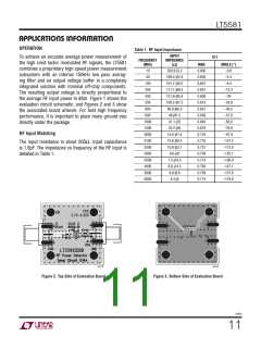
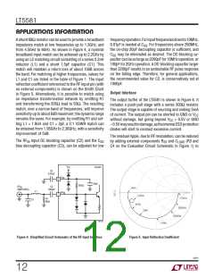
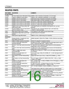
A shunt 68ꢀ resistor can be used to provide a broadband
impedance match at low frequencies up to 1.3GHz, and
from 4.5GHz to 6GHz. As shown in Figure 4, a nominal
broadband input match can be achieved up to 2.2GHz by
using an LC matching circuit consisting of a series 2.2nH
inductor (L1) and a shunt 1.5pF capacitor (C1). This
match will maintain a return loss of about 10dB across
the band. For matching at higher frequencies, values for
L1 and C1 are listed in the table of Figure 1. The input
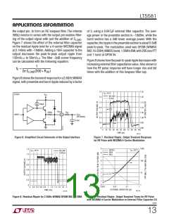
reflection coefficient referenced to the RF input pin (with
no external components) is shown on the Smith Chart
in Figure 5. Alternatively, it is possible to match using
an impedance transformation network by omitting R1
and transforming the 205ꢀ load to 50ꢀ. The resulting
match, over a narrow band of frequencies, will improve
sensitivity up to about 6dB maximumꢁ the dynamic range
remains the same. For example, by omitting R1 and set-
ting L1 = 1.8nH and C1 = 3pF, a 2:1 VSWR match can
be obtained from 1.95GHz to 2.36GHz, with a sensitivity
improvement of 5dB.
frequencyoperation.Forinputfrequenciesdownto10MHz,
0.01μF is needed at C . For frequencies above 250MHz,
SQ
the on-chip 20pF decoupling capacitor is sufficient, and
C
SQ
may be eliminated as desired. The DC-blocking ca-
pacitor can be as large as 2200pF for 10MHz operation, or
100pF for 2GHz operation. A DC-blocking capacitor larger
than 2200pF results in an undesirable RF pulse response
on the falling edge. Therefore, for general applications,
the recommended value for C2, is conservatively set at
1000pF.
Output Interface
The output buffer of the LT5581 is shown in Figure 6. It
includes a push-pull stage with a series 300ꢀ resistor.
The output stage is capable of sourcing and sinking 5mA
of current. The output pin can be shorted to GND or V
CC
without damage, but going beyond V + 0.5V or GND
CC
–0.5Vmayresultindamage,astheinternalESDprotection
diodes will start to conduct excessive current.
The residual ripple, due to RF modulation, can be reduced
The RF input DC blocking capacitor (C2) and the C
by adding external components R and C
(R3 and
IN
SQ
SS
LOAD
bias decoupling capacitor (C3), can be adjusted for low
C4 on the Evaluation Circuit Schematic in Figure 1) to
V
LT5581
CC
C3
0.01μF
C
SQ
8
7
20pF
205ꢀ
RF
C2
1000pF
IN
(MATCHED)
L1
RF
IN
R1
68ꢀ
C1
5581 F04
Figure 4. Simplified Circuit Schematic of the RF Input Interface
Figure 5. Input Reflection Coefficient
5581f
12

 Linear [ Linear ]