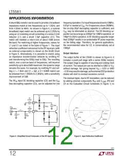
LT5581
APPLICATIONS INFORMATION
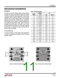
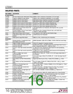
Figure 10 shows that rise time and fall time are strong
functions of RF input power. Data is taken without the
output filter capacitor.
peak envelope, divided by the total number of periodic
measurements in the measurement period). It is impor-
tant to note that the CF refers to the 150kHz low pass
filtered envelope of the signal. The error will depend on
the statistics and bandwidth of the modulation signal in
relation to the internal 150kHz filter. For example, in the
case of WCDMA, simulations prove that it is possible to
set the external filter capacitor corner frequency at 15kHz
and only introduce an error less than 0.1dB.
For a given RF modulation type—WCDMA, for exam-
ple—the internal 150kHz filter provides nominal filtering
of the residual ripple level. Additional external filtering
occurs in the log domain, which introduces a systematic
log error in relation to the signal’s crest factor, as shown
1
in the following equation in dB.
Figure 11 depicts the output AM modulation ripple as a
function of modulation difference frequency for a 2-tone
input signal at 2140MHz with –10dBm input power. The
–CF/10
Error|dB = 10 • log (r + (1 – r)10
) – CF • (r-1)
10
Where CF is the crest factor and r is the duty cycle of the
measurement (or number of measurements made at the
1
Steve Murray, “Beware of Spectrum Analyzer Power Averaging Techniques,” Microwaves
& RF, Dec. 2006.
9
30
25
20
15
10
5
0
T
= 25°C
A
T
= 25°C
A
8
7
6
5
4
3
2
1
0
FALL TIME
–0.5
–1.0
–1.5
–2.0
–2.5
–3.0
RISE TIME
0
–20 –15 –10 –5
INPUT POWER (dBm)
0
5
–30 –25
0.01
0.1
10
0.001
1
2-TONE FREQUENCY SEPARATION (MHz)
5581 F10
5581 F11
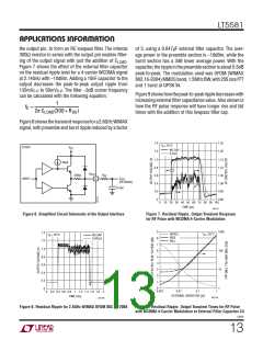
Figure 10. RF Pulse Response Rise Time
and Fall Time vs RF Input Power
Figure 11. Output DC Voltage Deviation and Residual
Ripple vs 2-Tone Separation Frequency
2.0
4.0
T
= 25°C
T
= 25°C
A
A
1.8
1.6
1.4
1.2
1.0
0.8
0.6
0.4
0.2
0
3.5
3.0
2.5
2.0
1.5
1.0
0.5
0
0dBm
–10dBm
–20dBm
–30dBm
NO RF INPUT
0dBm
–10dBm
–20dBm
–30dBm
NO RF INPUT
0.1
10
FREQUENCY (kHz)
100
1000
1
0.1
10
FREQUENCY (kHz)
100
1000
1
5581 F13
5581 F12
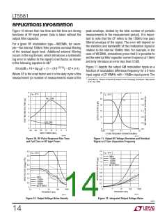
Figure 12. Output Voltage Noise Density
Figure 13. Integrated Output Voltage Noise
5581f
14

 Linear [ Linear ]