LT5581
APPLICATIONS INFORMATION
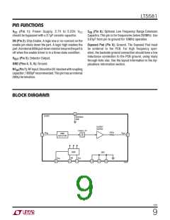
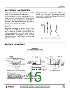
OPERATION
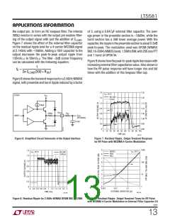
Table 1. RF Input Impedance
INPUT
S11
To achieve an accurate average power measurement of
the high crest factor modulated RF signals, the LT5581
combines a proprietary high speed power measurement
subsystem with an internal 150kHz low pass averag-
ing filter and an output voltage buffer in a completely
integrated solution with minimal off-chip components.
The resulting output voltage is directly proportional to
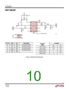
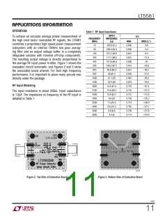
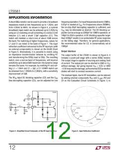
the average RF input power in dBm. Figure 1 shows the
evaluation circuit schematic, and Figures 2 and 3 show
the associated board artwork. For best high frequency
performance, it is important to place many ground vias
directly under the package.
FREQUENCY
(MHz)
IMPEDANCE
(Ω)
MAG
0.606
0.603
0.601
0.601
0.608
0.613
0.631
0.638
0.645
0.679
0.710
0.716
0.737
0.759
0.774
0.783
0.709
0.774
ANGLE (°)
–0.8
10
203.6-j5.5
199.5-j22.4
191.7-j40.3
171.1-j68.5
121.8-j95.4
100.2-j97.5
56.8-j86.5
48-j81.2
50
–3.4
100
–6.4
200
–12.3
–24
400
500
–29.8
–46.5
–51.8
–56.8
–79.5
–97.9
–101.2
–112.9
–125.7
–136.9
–147.1
–157.6
–179.9
800
900
1000
1500
2000
2100
2500
3000
3500
4000
5000
6000
41.1-j76
22.2-j55
RF Input Matching
14.6-j41.4
13.6-j39.2
10.8-j32.1
8.6-j25
The input resistance is about 205ꢀ. Input capacitance
is 1.6pF. The impedance vs frequency of the RF input is
detailed in Table 1.
7.3-j19.4
6.6-j14.5
8.8-j9.6
6.4-j0
5581 F02
5581 F03
Figure 2. Top Side of Evaluation Board
Figure 3. Bottom Side of Evaluation Board
5581f
11

 Linear [ Linear ]