LT5581
PIN FUNCTIONS
V
(Pin 1): Power Supply, 2.7V to 5.25V. V
C (Pin 8): Optional Low Frequency Range Extension
SQ
Capacitor. This pin is for frequencies below 250MHz. Use
0.01μF from pin to ground for 10MHz operation.
CC
CC
should be bypassed with a 0.1μF ceramic capacitor.
EN (Pin 2): Chip Enable. A logic low or no-connect on the
enable pin shuts down the part. A logic high enables the
part.Aninternal500kpull-downresistorensuresthepartis
off when the enable driver is in a three-state condition.
Exposed Pad (Pin 9): Ground. The Exposed Pad must
be soldered to the PCB. For high frequency oper-
ation, the backside ground connection should have a low
inductance connection to the PCB ground, using many
through-hole vias. See the layout information in the Ap-
plications Information section.
V
(Pin 3): Detector Output.
OUT
GND (Pins 4, 5, 6): Ground.
RF (Pin7):RFInput.ShouldbeDC-blockedwithcoupling
IN
capacitorꢁ 1000pF recommended. This pin has an internal
200ꢀ termination.
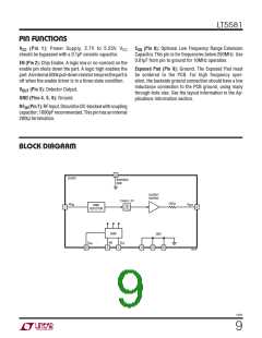
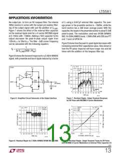
BLOCK DIAGRAM
9
LT5581
EXPOSED
PAD
OUTPUT
BUFFER
150kHz LPF
300ꢀ
RF
V
OUT
IN
RMS
DETECTOR
7
3
BIAS
EN
GND
C
V
CC
SQ
8
2
1
4
5
6
5581 BD
5581f
9

 Linear [ Linear ]