LT3580
APPLICATIONS INFORMATION
GND
GND
SYNC
1
2
3
4
8
7
6
5
9
C1
SYNC
1
2
3
4
8
7
6
5
9
V
IN
C1
SHDN
V
IN
L1
L2
SHDN
SW
L1
SW
C2
VIAS TO GROUND
PLANE REQUIRED
TO IMPROVE
D1
C2
VIAS TO GROUND
PLANE REQUIRED
TO IMPROVE
D1
C3
THERMAL
PERFORMANCE
3580 F09
THERMAL
V
OUT
PERFORMANCE
3580 F10
V
OUT
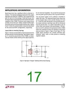
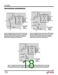
Figure 9. Suggested Component Placement for Boost Topology
(Both DFN and MSOP Packages. Not to Scale). Pin 9 (Exposed
Pad) must be soldered directly to the local ground plane for
adequate thermal performance. Multiple vias to additional
ground planes will improve thermal performance.
Figure 10. Suggested Component Placement for SEPIC Topology
(Both DFN and MSOP Packages. Not to Scale). Pin 9 (Exposed
Pad) must be soldered directly to the local ground plane for
adequate thermal performance. Multiple vias to additional
ground planes will improve thermal performance.
GND
SYNC
1
2
3
4
8
9
C1
7
V
IN
6
SHDN
5
L1
SW
C2
D1
L2
VIAS TO GROUND
PLANE REQUIRED
TO IMPROVE
C3
THERMAL
PERFORMANCE
3580 F11
V
OUT
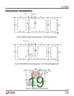
Figure 11. Suggested Component Placement for Inverting Topology (Both DFN and MSOP Packages. Not to Scale).
Note cut in ground copper at diode’s cathode. Pin 9 (Exposed Pad) must be soldered directly to local ground plane
for adequate thermal performance. Multiple vias to additional ground planes will improve thermal performance.
3580fc
18

 Linear [ Linear ]