LT1576/LT1576-5
TYPICAL PERFORMANCE CHARACTERISTICS
U W
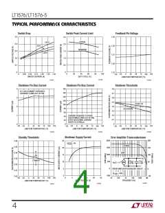
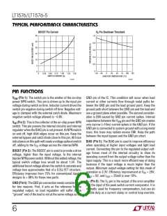
BOOST Pin Current
VC Pin Shutdown Threshold
30
25
20
15
10
5
1.0
0.8
0.6
0.4
0.2
0
0
–25
0
25
50
75
125
–50
100
0
0.50 0.75 1.00
1.25 1.50
0.25
SWITCH CURRENT (A)
JUNCTION TEMPERATURE (°C)
1576 G20
1576 G19
U
U
U
PIN FUNCTIONS
VSW (Pin 1): The switch pin is the emitter of the on-chip
power NPN switch. This pin is driven up to the input pin
voltage during switch on time. Inductor current drives the
switch pin negative during switch off time. Negative volt-
age is clamped with the external catch diode. Maximum
negative switch voltage allowed is –0.8V.
GND pin of the IC. This condition will occur when load
current or other currents flow through metal paths be-
tween the GND pin and the load ground point. Keep the
ground path short between the GND pin and the load and
use a ground plane when possible. The second consider-
ation is EMI caused by GND pin current spikes. Internal
capacitance between the VSW pin and the GND pin creates
very narrow (<10ns) current spikes in the GND pin. If the
GND pin is connected to system ground with a long metal
trace, this trace may radiate excess EMI. Keep the path
between the input bypass and the GND pin short.
VIN (Pin 2): This is the collector of the on-chip power NPN
switch. This pin powers the internal circuitry and internal
regulator when the BIAS pin is not present. At NPN switch
on and off, high dI/dt edges occur on this pin. Keep the
external bypass and catch diode close to this pin. All trace
inductanceonthispathwillcreateavoltagespikeatswitch
off, adding to the VCE voltage across the internal NPN.
BIAS (Pin 5): The BIAS pin is used to improve efficiency
when operating at higher input voltages and light load
current. Connecting this pin to the regulated output volt-
age forces most of the internal circuitry to draw its
operating current from the output voltage rather than the
input supply. This is a much more efficient way of doing
business if the input voltage is much higher than the
output. Minimum output voltage setting for this mode of
operation is 3.3V. Efficiency improvement at VIN = 20V,
VOUT = 5V, and IOUT = 25mA is over 10%.
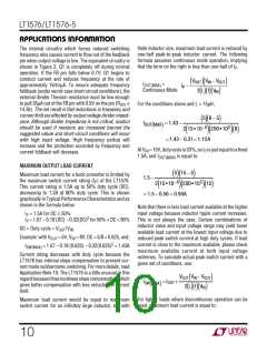
BOOST (Pin 3): The BOOST pin is used to provide a drive
voltage, higher than the input voltage, to the internal
bipolarNPNpowerswitch. Withoutthisaddedvoltage, the
typical switch voltage loss would be about 1.5V. The
additional boost voltage allows the switch to saturate and
voltage loss approximates that of a 0.2Ω FET structure.
Efficiency improves from 75% for conventional bipolar
designs to > 88% for these new parts.
VC (Pin 6): The VC pin is the output of the error amplifier
and the input of the peak switch current comparator. It is
normally used for frequency compensation, but can do
double duty as a current clamp or control loop override.
GND(Pin4):TheGNDpinconnectionneedsconsideration
for two reasons. First, it acts as the reference for the
regulated output, so load regulation will suffer if the
“ground” end of the load is not at the same voltage as the
6

 Linear [ Linear ]