LT1576/LT1576-5
W W U W
U
W U
ABSOLUTE MAXIMUM RATINGS
(Note 1)
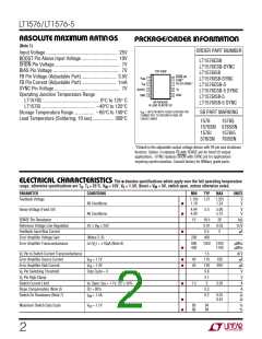
PACKAGE/ORDER INFORMATION
ORDER PART NUMBER
Input Voltage .......................................................... 25V
BOOST Pin Above Input Voltage ............................. 10V
SHDN Pin Voltage..................................................... 7V
BIAS Pin Voltage ...................................................... 7V
FB Pin Voltage (Adjustable Part)............................ 3.5V
FB Pin Current (Adjustable Part)............................ 1mA
SYNC Pin Voltage ..................................................... 7V
Operating Junction Temperature Range
LT1576C............................................... 0°C to 125° C
LT1576I ........................................... –40°C to 125°C
Storage Temperature Range ................ –65°C to 150°C
Lead Temperature (Soldering, 10 sec)................. 300°C
LT1576CS8
LT1576CS8-SYNC
TOP VIEW
LT1576IS8
SHDN OR
1
2
3
4
8
7
6
5
V
SW
LT1576IS8-SYNC
LT1576CS8-5
SYNC*
FB OR SENSE*
V
IN
V
C
BOOST
GND
LT1576CS8-5 SYNC
LT1576IS8-5
LT1576IS8-5 SYNC
BIAS
S8 PACKAGE
8-LEAD PLASTIC SO
θJA = 80°C/ W WITH FUSED GROUND PIN
CONNECTED TO GROUND PLANE OR
LARGE LANDS
S8 PART MARKING
1576
1576SN 5765SN
1576I 1576I5
576ISN 76I5SN
15765
*Default is the adjustable output voltage device with FB pin and shutdown
function. Option -5 replaces FB with SENSE pin for fixed 5V output
applications. -SYNC replaces SHDN with SYNC pin for applications
requiring synchronization. Consult factory for Military grade parts.
The ● denotes specifications which apply over the full operating temperature
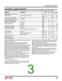
ELECTRICAL CHARACTERISTICS
range, otherwise specifications are TA, TJ = 25°C, VIN = 15V, VC = 1.5V, Boost = VIN + 5V, switch open, unless otherwise noted.
PARAMETER
CONDITIONS
All Conditions
All Conditions
MIN
TYP
MAX
UNITS
Feedback Voltage
1.195 1.21
1.18
1.225
1.24
V
V
●
●
Sense Voltage (Fixed 5V)
4.94
4.90
5.0
5.06
5.10
V
V
SENSE Pin Resistance
13
18.5
0.01
0.5
26
0.03
2
kΩ
%/V
µA
Reference Voltage Line Regulation
Feedback Input Bias Current
Error Amplifier Voltage Gain
Error Amplifier Transconductance
5V ≤ V ≤ 25V
IN
●
●
(Notes 2, 8)
200
400
∆I (V ) = ±10µA (Note 8)
800
400
1050
1300
1700
µMho
µMho
C
V Pin to Switch Current Transconductance
1.5
110
130
0.8
2.1
2
A/V
µA
µA
V
C
Error Amplifier Source Current
Error Amplifier Sink Current
V
V
= 1.1V
= 1.4V
●
●
40
50
190
200
FB
FB
V Pin Switching Threshold
C
Duty Cycle = 0
V Pin High Clamp
C
V
Switch Current Limit
V Open, V = 1.1V, DC ≤ 50%
C
●
1.5
3.50
A
FB
Slope Compensation (Note 9)
Switch On Resistance (Note 7)
DC = 80%
0.3
0.2
A
I
= 1.5A
0.35
0.45
Ω
Ω
SW
●
●
Maximum Switch Duty Cycle
V
FB
= 1.1V
90
86
94
94
%
%
2

 Linear [ Linear ]