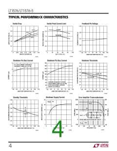
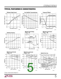
LT1576/LT1576-5
W
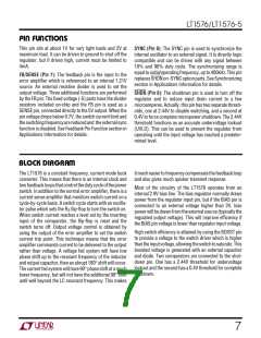
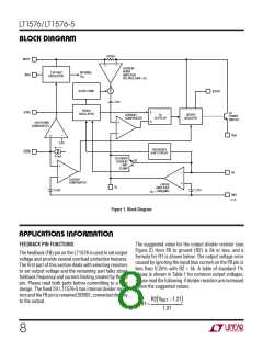
BLOCK DIAGRAM
0.025Ω
INPUT
+
–
CURRENT
SENSE
2.9V BIAS
REGULATOR
INTERNAL
CC
BIAS
AMPLIFIER
VOLTAGE GAIN = 35
V
SLOPE COMP
BOOST
Σ
0.8V
200kHz
OSCILLATOR
S
R
SYNC
Q1
POWER
SWITCH
R
DRIVER
CIRCUITRY
CURRENT
COMPARATOR
S
FLIP-FLOP
+
–
SHUTDOWN
COMPARATOR
–
+
V
SW
0.4V
FREQUENCY
SHDN
SHIFT CIRCUIT
3.5µA
FOLDBACK
CURRENT
LIMIT
Q2
+
–
CLAMP
–
FB
LOCKOUT
COMPARATOR
+
ERROR
V
C
AMPLIFIER
2.44V
1.21V
g
= 1000µMho
m
GND
1576 BD
Figure 1. Block Diagram
U
W U U
APPLICATIONS INFORMATION
FEEDBACK PIN FUNCTIONS
The suggested value for the output divider resistor (see
Figure 2) from FB to ground (R2) is 5k or less, and a
formula for R1 is shown below. The output voltage error
caused by ignoring the input bias current on the FB pin is
less than 0.25% with R2 = 5k. A table of standard 1%
values is shown in Table 1 for common output voltages.
Please read the following if divider resistors are increased
above the suggested values.
The feedback (FB) pin on the LT1576 is used to set output
voltage and provide several overload protection features.
The first part of this section deals with selecting resistors
to set output voltage and the remaining part talks about
foldback frequency and current limiting created by the FB
pin. Please read both parts before committing to a final
design. The fixed 5V LT1576-5 has internal divider resis-
tors and the FB pin is renamed SENSE, connected directly
to the output.
R2 VOUT −1.21
(
)
R1=
1.21
8

 Linear [ Linear ]