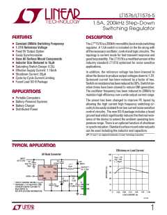
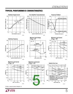
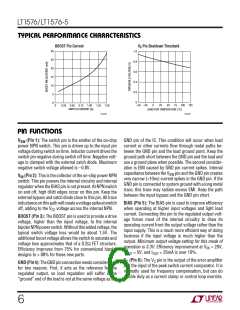
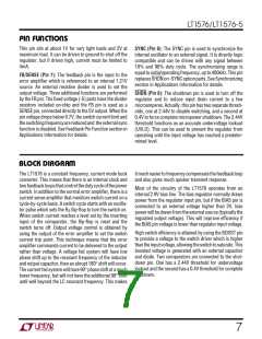
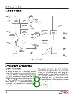
LT1576/LT1576-5
The ● denotes specifications which apply over the full operating temperature
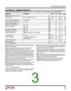
ELECTRICAL CHARACTERISTICS
range, otherwise specifications are TA, TJ = 25°C, VIN = 15V, VC = 1.5V, Boost = VIN + 5V, switch open, unless otherwise noted.
PARAMETER
CONDITIONS
V Set to Give 50% Duty Cycle
MIN
TYP
8
MAX
UNITS
Minimum Switch Duty Cycle (Note 10)
Switch Frequency
%
180
160
200
220
240
kHz
kHz
C
●
●
●
●
●
Switch Frequency Line Regulation
Frequency Shifting Threshold on FB Pin
Minimum Input Voltage (Note 3)
Minimum Boost Voltage (Note 4)
Boost Current (Note 5)
5V ≤ V ≤ 25V
0
0.15
1.0
5.5
3.0
%/V
V
IN
∆f = 10kHz
0.4
0.74
5.0
2.3
V
I
≤ 1.5A
V
SW
I
I
= 0.5A
= 1.5A
●
●
9
27
18
50
mA
mA
SW
SW
V
Supply Current (Note 6)
V
V
V
= 5V
= 5V
●
●
0.55
1.6
20
0.8
2.2
mA
mA
IN
BIAS
BIAS
SHDN
BIAS Supply Current (Note 6)
Shutdown Supply Current
= 0V, V ≤ 25V, V = 0V, V Open
50
75
µA
µA
IN
SW
C
●
●
Lockout Threshold
V Open
C
2.34
2.42
2.50
V
Shutdown Thresholds
V Open Device Shutting Down
Device Starting Up
●
●
0.13
0.25
0.37
0.45
0.60
0.7
V
V
C
Synchronization Threshold
Synchronizing Range
1.5
2.2
V
kHz
kΩ
250
400
SYNC Pin Input Resistance
40
Note 1: Absolute Maximum Ratings are those values beyond which the life
Note 7: Switch on resistance is calculated by dividing V to V voltage
IN SW
by the forced current (1.5A). See Typical Performance Characteristics for
the graph of switch voltage at other currents.
of a device may be impaired.
Note 2: Gain is measured with a V swing equal to 200mV above the
C
switching threshold level to 200mV below the upper clamp level.
Note 8: Transconductance and voltage gain refer to the internal amplifier
exclusive of the voltage divider. To calculate gain and transconductance,
refer to the SENSE pin on the fixed voltage parts. Divide values shown by
Note 3: Minimum input voltage is not measured directly, but is guaranteed
by other tests. It is defined as the voltage where internal bias lines are still
regulated so that the reference voltage and oscillator frequency remain
constant. Actual minimum input voltage to maintain a regulated output will
depend on output voltage and load current. See Applications Information.
Note 4: This is the minimum voltage across the boost capacitor needed to
guarantee full saturation of the internal power switch.
the ratio V /1.21.
OUT
Note 9: Slope compensation is the current subtracted from the switch
current limit at 80% duty cycle. See Maximum Output Load Current in the
Applications Information section for further details.
Note 10: Minimum on-time is 400ns typical. For a 200kHz operating
frequency this means the minimum duty cycle is 8%. In frequency
foldback mode, the effective duty cycle will be less than 8%.
Note 5: Boost current is the current flowing into the boost pin with the pin
held 5V above input voltage. It flows only during switch on time.
Note 6: V supply current is the current drawn when the BIAS pin is held
IN
at 5V and switching is disabled. Total input referred supply current is
calculated by summing input supply current (I ) with a fraction of BIAS
SI
supply current (I
)
SB
I
= I + (I )(V
/V )(1.15)
BIAS IN
TOT
SI
SB
with V = 15V, V
= 5V, I = 0.55mA, I = 1.6mA and I
= 1.16mA.
IN
BIAS
SI
SB
TOT
If the BIAS pin is unavailable or open circuit, the sum of V and BIAS
IN
supply currents will be drawn by the V pin.
IN
3

 Linear [ Linear ]