LT1576/LT1576-5
U
W U U
APPLICATIONS INFORMATION
finite inductor size, maximum load current is reduced by
one-half peak-to-peak inductor current. The following
formula assumes continuous mode operation, implying
that the term on the right is less than one-half of IP.
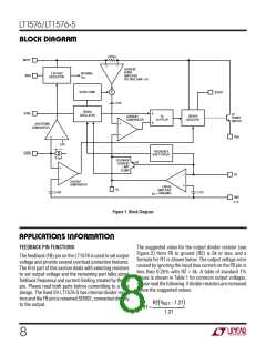
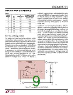
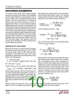
The internal circuitry which forces reduced switching
frequency also causes current to flow out of the feedback
pin when output voltage is low. The equivalent circuitry is
shown in Figure 2. Q1 is completely off during normal
operation. If the FB pin falls below 0.7V, Q1 begins to
conduct current and reduces frequency at the rate of
approximately 1kHz/µA. To ensure adequate frequency
foldback (under worst-case short-circuit conditions), the
external divider Thevinin resistance must be low enough
VOUT V − VOUT
(
)( IN
)
IOUT(MAX)
=
IP −
Continuous Mode
2 L f V
( )( )( IN
)
to pull 35µA out of the FB pin with 0.5V on the pin (RDIV
≤
For the conditions above and L = 15µH,
14.3k). The net result is that reductions in frequency and
current limit are affected by output voltage divider imped-
ance. Although divider impedance is not critical, caution
should be used if resistors are increased beyond the
suggested values and short-circuit conditions will occur
with high input voltage. High frequency pickup will
increase and the protection accorded by frequency and
current foldback will decrease.
5 8 − 5
( )(
)
IOUT MAX) = 1.43 −
(
2 15 •10−6 200•103
8
( )
(
)(
)
=1.43 − 0.31= 1.12A
AtVIN =15V, dutycycleis33%, soIP isjustequaltoafixed
1.5A, and IOUT(MAX) is equal to:
MAXIMUM OUTPUT LOAD CURRENT
5 15 − 5
( )(
)
Maximum load current for a buck converter is limited by
the maximum switch current rating (IP) of the LT1576.
This current rating is 1.5A up to 50% duty cycle (DC),
decreasing to 1.3A at 80% duty cycle. This is shown
graphically in Typical Performance Characteristics and as
shown in the formula below:
1.5 −
2 15 •10−6 200•103 15
( )
(
)(
)
= 1.5 − 0.56 = 0.94A
Note that there is less load current available at the higher
input voltage because inductor ripple current increases.
This is not always the case. Certain combinations of
inductor value and input voltage range may yield lower
available load current at the lowest input voltage due to
reduced peak switch current at high duty cycles. If load
current is close to the maximum available, please check
maximum available current at both input voltage
extremes. To calculate actual peak switch current with a
given set of conditions, use:
IP = 1.5A for DC ≤ 50%
IP = 1.67 – 0.18 (DC) – 0.32(DC)2 for 50% < DC < 90%
DC = Duty cycle = VOUT/VIN
Example: with VOUT = 5V, VIN = 8V; DC = 5/8 = 0.625, and;
ISW(MAX) = 1.67 – 0.18 (0.625) – 0.32(0.625)2 = 1.43A
Current rating decreases with duty cycle because the
LT1576 has internal slope compensation to prevent cur-
rent mode subharmonic switching. For more details, read
Application Note 19. The LT1576 is a little unusual in this
regardbecauseithasnonlinearslopecompensationwhich
gives better compensation with less reduction in current
limit.
VOUT V − VOUT
(
IN
)
ISW PEAK =IOUT
+
(
)
2 L f V
( )( )( IN
)
For lighter loads where discontinuous operation can be
used, maximum load current is equal to:
Maximum load current would be equal to maximum
switch current for an infinitely large inductor, but with
10

 Linear [ Linear ]