LT1510/LT1510-5
U
W U U
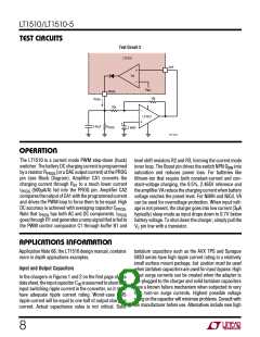
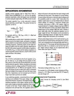
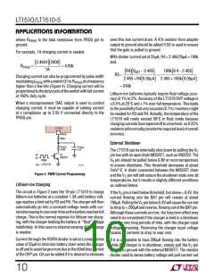
APPLICATIONS INFORMATION
90
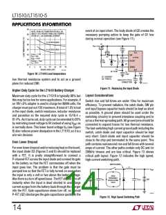
event of an input short. The body diode of Q2 creates the
necessary pumping action to keep the gate of Q1 low
during normal operation (see Figure 11).
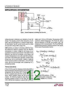
NOTE: PEAK DIE TEMPERATURE WILL BE
ABOUT 10°C HIGHER THAN LEAD TEMPER-
80
ATURE AT 1.3A CHARGING CURRENT
70
2-LAYER BOARD
60
Q1
V
IN
+
4-LAYER BOARD
50
40
30
20
V
CC
I
= 1.3A
CHRG
IN
BAT
SW
V
V
V
= 16V
Q2
LT1510
C3
D2
= 8.4V
= V
R
X
BOOST
BOOST
= 25°C
BAT
D1
L1
50k
T
A
0
5
10
15
20
BOARD AREA (IN2)
25
30
35
SENSE
V
1510 F09
X
BAT
3V TO 6V
C
X
V
BAT
Figure 10. LT1510 Lead temperature
10µF
Q1: Si4435DY
Q2: TP0610L
+
low thermal resistance system and to act as a ground
plane for reduced EMI.
HIGH DUTY CYCLE
CONNECTION
1510 F10
Figure 11. Replacing the Input Diode
Higher Duty Cycle for the LT1510 Battery Charger
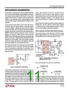
Layout Considerations
Maximum duty cycle for the LT1510 is typically 90% but
this may be too low for some applications. For example, if
an 18V ±3% adapter is used to charge ten NiMH cells, the
charger must put out 15V maximum. A total of 1.6V is lost
in the input diode, switch resistance, inductor resistance
and parasitics so the required duty cycle is 15/16.4 =
91.4%. As it turns out, duty cycle can be extended to 93%
by restricting boost voltage to 5V instead of using VBAT as
is normally done. This lower boost voltage VX (see Figure
8) also reduces power dissipation in the LT1510, so it is a
win-win decision.
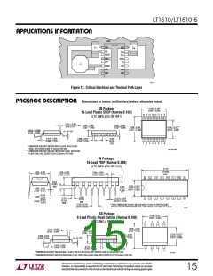
Switch rise and fall times are under 10ns for maximum
efficiency. To prevent radiation, the catch diode, SW pin
and input bypass capacitor leads should be kept as short
as possible. A ground plane should be used under the
switching circuitry to prevent interplane coupling and to
act as a thermal spreading path. All ground pins should be
connected to expand traces for low thermal resistance.
The fast-switching high current ground path including the
switch, catch diode and input capacitor should be kept
very short. Catch diode and input capacitor should be
close to the chip and terminated to the same point. This
path contains nanosecond rise and fall times with several
amps of current. The other paths contain only DC and /or
200kHz triwave and are less critical. Figure 13 shows
critical path layout. Figure 12 indicates the high speed,
high current switching path.
Even Lower Dropout
Forevenlowerdropoutand/orreducingheatontheboard,
the input diode D3 (Figures 2 and 6) should be replaced
with a FET. It is pretty straightforward to connect a
P-channel FET across the input diode and connect its gate
to the battery so that the FET commutates off when the
input goes low. The problem is that the gate must be
pumped low so that the FET is fully turned on even when
the input is only a volt or two above the battery voltage.
Alsothereisaturnoffspeedissue. TheFETshouldturnoff
instantly when the input is dead shorted to avoid large
current surges form the battery back through the charger
into the FET. Gate capacitance slows turn off, so a small
P-FET (Q2) discharges the gate capacitance quickly in the
SWITCH NODE
L1
V
BAT
HIGH
FREQUENCY
CIRCULATING
PATH
C
C
OUT
V
IN
BAT
IN
1510 F12
Figure 12. High Speed Switching Path
14

 Linear [ Linear ]