LT1108
U
O
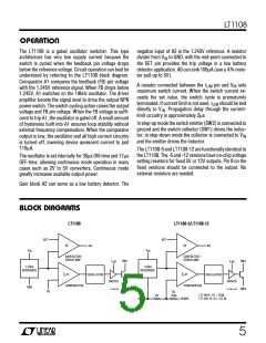
1 OPERATI
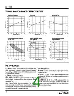
The LT1108 is a gated oscillator switcher. This type
architecture has very low supply current because the
switch is cycled when the feedback pin voltage drops
below the reference voltage. Circuit operation can best be
understood by referring to the LT1108 block diagram.
Comparator A1 compares the feedback (FB) pin voltage
with the 1.245V reference signal. When FB drops below
1.245V, A1 switches on the 19kHz oscillator. The driver
amplifier boosts the signal level to drive the output NPN
power switch. The switch cycling action raises the output
voltage and FB pin voltage. When the FB voltage is suffi-
cient to trip A1, the oscillator is gated off. A small amount
of hysteresis built into A1 ensures loop stability without
external frequency compensation. When the comparator
output is low, the oscillator and all high current circuitry
is turned off, lowering device quiescent current to just
110µA.
negative input of A2 is the 1.245V reference. A resistor
divider from VIN to GND, with the mid-point connected to
the SET pin provides the trip voltage in a low battery
detector application. A0 can sink 100µA (use a 47k resis-
tor pull-up to 5V).
A resistor connected between the ILIM pin and VIN sets
maximum switch current. When the switch current ex-
ceeds the set value, the switch cycle is prematurely
terminated. If current limit is not used, ILIM should be tied
directly to VIN. Propagation delay through the current-
limit circuitry is approximately 2µs.
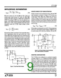
In step-up mode the switch emitter (SW2) is connected to
ground and the switch collector (SW1) drives the induc-
tor; in step-down mode the collector is connected to VIN
and the emitter drives the inductor.
The LT1108-5 and LT1108-12 are functionally identical to
the LT1108. The -5 and -12 versions have on-chip voltage
setting resistors for fixed 5V or 12V outputs. Pin 8 on the
fixed versions should be connected to the output. No
external resistors are needed.
The oscillator is set internally for 36µs ON-time and 17µs
OFF-time, allowing continuous mode operation in many
cases such as 2V to 5V converters. Continuous mode
greatly increases available output power.
Gain block A2 can serve as a low battery detector. The
W
BLOCK DIAGRA S
LT1108
LT1108-5/LT1108-12
SET
SET
A2
A2
A0
A0
V
IN
V
IN
GAIN BLOCK/
ERROR AMP
GAIN BLOCK/
ERROR AMP
I
SW1
SW2
I
SW1
SW2
LIM
LIM
1.245V
REFERENCE
1.245V
REFERENCE
A1
A1
OSCILLATOR
OSCILLATOR
DRIVER
DRIVER
COMPARATOR
COMPARATOR
GND
LT1108 • BD
LT1108-5 • BD
FB
R2
753k
R1
LT1108-5: R1 = 250k
LT1108-12: R1 = 87.4k
GND
SENSE
5

 Linear [ Linear ]