LT1108
TYPICAL PERFOR A CE CHARACTERISTICS
U W
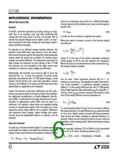
Oscillator Frequency
Duty Cycle
Switch-ON Time
80
75
70
65
60
55
50
22
21
20
19
18
17
16
15
14
44
42
40
38
36
34
32
30
13
–25
0
50
–50
75
100
25
–25
0
50
–50 –25
0
25
50
75
100
–50
75
100
25
TEMPERATURE (°C)
TEMPERATURE (°C)
TEMPERATURE (˚C)
LT1108 • TPC08
LT1108 • TPC07
LT1108 • TPC09
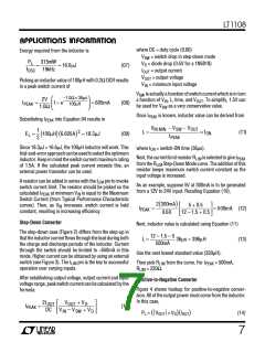
Minimum/Maximum Frequency
vs ON-Time
Switch Saturation Voltage
Step-Up Mode
Switch Saturation Voltage
Step-Down Mode
28
1.8
1.7
0.8
0.7
0.6
0.5
I
= 650mA
SW
I
= 650mA
SW
26
24
22
20
18
16
14
12
10
0
1.6
1.5
1.4
0.4
0.3
1.3
1.2
1.1
1.0
0.9
0.8
0.2
0.1
0
25
30
35
40
45
50
–25
0
50
–50 –25
25
50
75
100
–50
75
100
25
0
ON-TIME (µs)
TEMPERATURE (°C)
TEMPERATURE (°C)
LT1108 • TPC10
LT1108 • TPC11
LT1108 • TPC12
U
O
U
U
PI
FU CTI
S
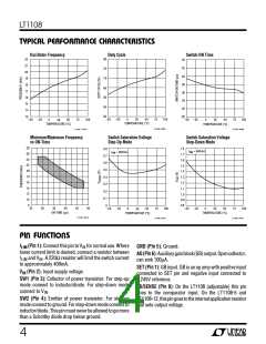
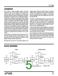
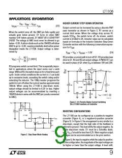
ILIM (Pin 1): Connect this pin to VIN for normal use. Where
lower current limit is desired, connect a resistor between
ILIM and VIN. A 220Ω resistor will limit the switch current
to approximately 400mA.
GND (Pin 5): Ground.
AO(Pin6):Auxiliarygainblock(GB)output.Opencollector,
can sink 100µA.
SET (Pin 7): GB input. GB is an op amp with positive input
connected to SET pin and negative input connected to
1.245V reference.
FB/SENSE (Pin 8): On the LT1108 (adjustable) this pin
goes to the comparator input. On the LT1108-5 and
LT1108-12,thispingoestotheinternalapplicationresistor
that sets output voltage.
VIN (Pin 2): Input supply voltage.
SW1 (Pin 3): Collector of power transistor. For step-up
mode connect to inductor/diode. For step-down mode
connect to VIN.
SW2 (Pin 4): Emitter of power transistor. For step-up
mode connect to ground. For step-down mode connect to
inductor/diode. Thispinmustneverbeallowedtogomore
than a Schottky diode drop below ground.
4

 Linear [ Linear ]