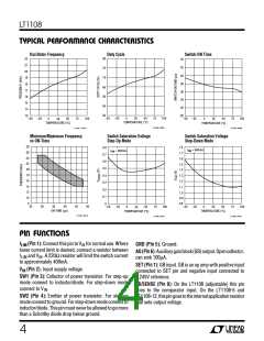
LT1108
O U
W
U
PPLICATI
A
S I FOR ATIO
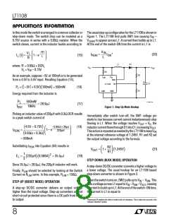
HIGHER CURRENT STEP-DOWN OPERATION
V
− V − V
IN
SW
OUT
I
=
t
(22)
PEAK
ON
L
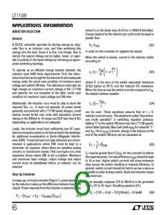
Output current can be increased by using a discrete PNP
pass transistor as shown in Figure 3. R1 serves as a
current limit sense. When the voltage drop across R1
equals 0.5VBE, the switch turns off. As shown, switch
current is limited to 2A. Inductor value can be calculated
based on formulas in the Inductor Selection Step-Down
Converter section with the following conservative expres-
When the switch turns off, the SW2 pin falls rapidly and
actually goes below ground. D1 turns on when SW2
reaches 0.4V below ground. D1 MUST BE A SCHOTTKY
DIODE. The voltage at SW2 must never be allowed to go
below –0.5V. A silicon diode such as the 1N4933 will allow
SW2 to go to –0.8V, causing potentially destructive power
dissipation inside the LT1108. Output voltage is deter-
mined by
sion for VSW
= V + V ≈ 1.0V
Q1SAT
:
V
(24)
SW
R1
R2 provides a current path to turn off Q1. R3 provides base
drive to Q1. R4 and R5 set output voltage. A PMOS FET can
be used in place of Q1 when VIN is between 10V and 20V.
R2
R1
V
= 1+
1.245V
(23)
(
)
OUT
R3 programs switch current limit. This is especially impor-
tant in applications where the input varies over a wide
range. Without R3, the switch stays on for a fixed time each
cycle. Under certain conditions the current in L1 can build
up to excessive levels, exceeding the switch rating and/or
saturating the inductor. The 100Ω resistor programs the
switch to turn off when the current reaches approximately
700mA. When using the LT1108 in step-down mode,
output voltage should be limited to 6.2V or less. Higher
output voltages can be accommodated by inserting a
1N5818 diode in series with the SW2 pin (anode connected
to SW2).
R1
Q1
V
L1
0.15Ω
ZETEX ZTX749
IN
30V
V
OUT
MAX
R2
100Ω
R6
100Ω
D1
1N5821
R3
330Ω
V
I
L
SW1
IN
+
+
C2
C1
LT1108
R4
FB
SW2
GND
R5
R4
V
= 1.245V 1 +
(
)
OUT
R5
LT1108 • F03
Figure 3. Q1 Permits Higher Current Switching
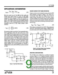
The LT1108 Functions as Controller
V
IN
R3
100Ω
+
I
V
IN
SW1
FB
LIM
C2
INVERTING CONFIGURATIONS
LT1108
GND
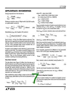
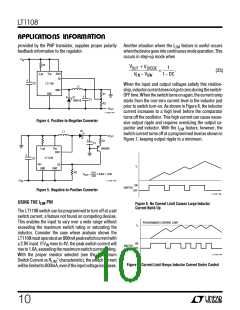
The LT1108 can be configured as a positive-to-negative
converter (Figure 4), or a negative-to-positive converter
(Figure 5). In Figure 4, the arrangement is very similar to a
step-down, except that the high side of the feedback is
referred to ground. This level shifts the output negative. As
in the step-down mode, D1 must be a Schottky diode,
and VOUT should be less than 6.2V. More negative output
voltages can be accommodated as in the prior section.
L1
V
SW2
OUT
R2
R1
+
D1
1N5818
C1
LT1108 • F02
Figure 2. Step-Down Mode Hookup
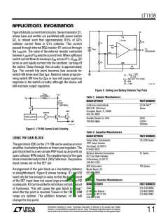
InFigure5, theinputisnegativewhiletheoutputispositive.
Inthisconfiguration,themagnitudeoftheinputvoltagecan
be higher or lower than the output voltage. A level shift,
9

 Linear [ Linear ]