LT3587
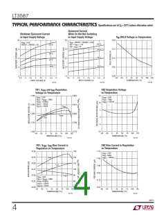
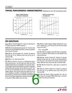
TYPICAL PERFORMANCE CHARACTERISTICS Specifications are at T = 25°C unless otherwise noted.
A
EN/SS1, EN/SS3 Shutdown
Threshold vs Temperature
CAP3 Overvoltage Clamp
vs Temperature
0.45
0.40
0.35
0.30
0.25
0.20
31
30
29
28
27
V
= 3.6V
V
VIN
= 3.6V
VIN
–50 –25
0
25
50
75 100 125
–50 –25
0
25
50
75 100 125
TEMPERATURE (°C)
TEMPERATURE (°C)
3587 G17
3587 G18
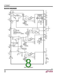
PIN FUNCTIONS
V
(Pin 1): Boost3 Output Pin. This pin is the drain of
FB2 (Pin 6): Inverter Output Voltage Feedback Pin. Con-
nect a resistor R from this pin to the Inverter Output
OUT3
an output disconnect PMOS transistor.
FB2
(V ) such that:
NEG
CAP3 (Pin 2): Boost3 Output Capacitor Pin. This pin is the
sourceofanoutputPMOSdisconnect.Connectacapacitor
from this pin to ground.
R
= |V |/8μA
NEG
FB2
Note that FB2 pin voltage is about 0V when in regulation.
There is an internal 153k resistor from the FB2 pin to the
internal reference.
SW3 (Pin 3): Boost3 Switch Pin. Connect an inductor
from this pin to V . Minimize trace area at this pin to
IN
minimize EMI.
SW2 (Pin 9): Inverter Switch Pin. Connect an inductor
GND (Pin 4, 7, 8, 12): Ground Pins.
between this pin and V , as well as the flying capacitor
IN
from this pin to the anode of the lnverter ground return
FLT (Pin 5): Fault Pin. This pin is a bidirectional open-
drain pull-down pin. This pin pulls low when any of the
enabled outputs fall out of regulation for more than 16ms.
Each output is ignored during start-up until its respective
enable/soft-start pin allows for full inductor current. This
pin can also be externally forced low to disable all the
supply outputs. Once this pin goes low (either due to an
out of regulation condition or externally forced low), the
pin latches low until the inputs to EN/SS1 and EN/SS3 are
set low or the input supply pin is recycled. Pull up this pin
diode. Minimize trace area at this pin to minimize EMI.
NC (Pin 10): No Connect Pin. Leave open or connect to
ground.
SW1 (Pin 11): Boost1 Switch Pin. Connect an inductor
from this pin to V . Minimize trace area at this pin to
IN
minimize EMI.
CAP1 (Pin 13): Boost1 Output Capacitor Pin. This pin
is the source of an output PMOS disconnect. Connect a
capacitor from this pin to ground.
to V with a 200k resistor when not used.
IN
3587fc
6

 Linear [ Linear ]