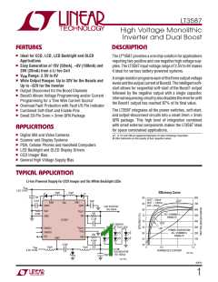
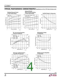
LT3587
ABSOLUTE MAXIMUM RATINGS
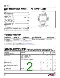
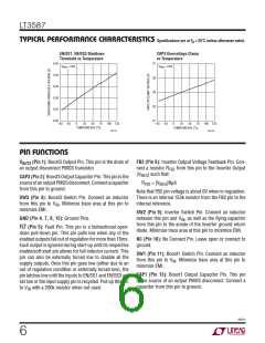
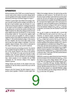
PIN CONFIGURATION
(Note 1)
TOP VIEW
V ..............................................................................6V
IN
Soft-Start Input Pins
20 19 18 17 16
EN/SS1, EN/SS3 .....................................................6V
Feedback Pins
FB1
V
15
14
13
12
11
V
1
2
3
4
5
OUT3
CAP3
SW3
GND
FLT
OUT1
FB1, FB2, I , V ................................. –0.2V to 6V
FB3 FB3
CAP1
GND
SW1
21
8
High Voltage Switch Pins
SW1, SW2, SW3...................................................40V
High Voltage Output Pins
6
7
9 10
CAP1, CAP3, V
, V
...................................32V
OUT1 OUT3
Bidirectional I/O Pin
UD PACKAGE
20-LEAD (3mm s 3mm) PLASTIC QFN
= 68°C/W, θ = 4.2°C/W
FLT..........................................................................6V
FLT Current ........................................................10mA
Operating Junction Temperature Range.. –40°C to 125°C
Storage Temperature Range...................–65°C to 125°C
θ
JA
JC
EXPOSED PAD (PIN 21) IS GND, MUST BE SOLDERED TO PCB
ORDER INFORMATION
LEAD FREE FINISH
TAPE AND REEL
PART MARKING
PACKAGE DESCRIPTION
20-Lead (3mm × 3mm) Plastic QFN
TEMPERATURE RANGE
–40°C to 125°C
LT3587EUD#PBF
LT3587EUD#TRPBF
LDNC
Consult LTC Marketing for parts specified with wider operating temperature ranges.
Consult LTC Marketing for information on non-standard lead based finish parts.
For more information on lead free part marking, go to: http://www.linear.com/leadfree/
For more information on tape and reel specifications, go to: http://www.linear.com/tapeandreel/
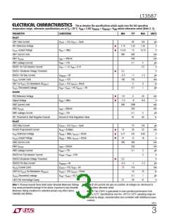
ELECTRICAL CHARACTERISTICS
The l denotes the specifications which apply over the full operating
temperature range, otherwise specifications are at TA = 25°C. VVIN = 3.6V, VEN/SS1 = VEN/SS3 = VVIN unless otherwise noted (Note 2, 3).
PARAMETER
CONDITIONS
MIN
TYP
MAX
UNITS
V
Operating Input Voltage Range
Quiescent Current
2.5
6
4
V
V
V
= 0V, V
= V OR
2.4
mA
EN/SS1
EN/SS1
EN/SS1
EN/SS3
VIN
= V , V
= 0V OR
VIN EN/SS3
= V
= V
VIN
EN/SS3
Not Switching
V
= V
= 0V, In Shutdown
5.5
1
9
μA
MHz
%
EN/SS1
EN/SS3
l
l
Switching Frequency
0.8
87
1.2
Maximum Duty Cycle
93
50
16
1.0
Minimum On Time
70
ns
Power Fault Delay from Any Output to FLT
FLT Input Threshold Low
FLT Leakage Current
ms
V
l
l
l
0.4
1.6
1
V
FLT
= 5V
μA
V
FLT Voltage Output Low
I
FLT
= 1mA
0.4
3587fc
2

 Linear [ Linear ]