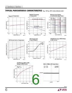
LT3694/LT3694-1
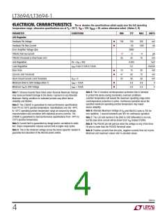
ELECTRICAL CHARACTERISTICS The l denotes the specifications which apply over the full operating
temperature range, otherwise specifications are at TA = 25°C, VIN = 12V, VBIAS = 3V, unless otherwise noted. (Notes 2, 9)
PARAMETER
Internal Undervoltage Lockout
CONDITIONS
MIN
3.5
36
TYP
3.8
38
MAX
4
UNITS
V
l
l
V
IN
Overvoltage Shutdown Threshold
Input Quiescent Current
40
2
V
Not Switching
Not Switching
1
mA
mA
µA
mV
V
Bias Quiescent Current
2
3.5
2
Shutdown Current
V
= 0.1V
0.1
500
1.2
0.01
1.0
EN/UVLO
EN/UVLO Threshold, Bias On
EN/UVLO Threshold, Switching On
Reference Voltage Line Regulation
Switching Frequency
350
l
1.16
1.23
5V < V < 36V
%/V
MHz
MHz
V
IN
l
l
l
l
l
l
R = 40.2k
T
0.9
0.25
1.5
1.1
2.5
SYNC Input Frequency Range
LT3694 Only
LT3694 Only
LT3694 Only
V , SYNC
IH
V , SYNC
IL
0.35
2.6
V
V
V
, CLKOUT
I
I
I
= –50µA, LT3694-1 Only
= 50µA, LT3694-1 Only
= 250µA
1.6
V
OH
CLKOUT
CLKOUT
PGOOD
, CLKOUT
0.3
V
OL
PGOOD Output Voltage Low
PGOOD Leakage
0.2
10
90
0.4
V
V
= 2V
1000
94
nA
%
PGOOD
PGOOD Threshold (Relative to V
Switching Regulator
)
(Note 8)
86
FB
l
l
Feedback Pin Voltage
735
750
–50
350
600
–3
765
mV
nA
µS
V/V
µA
mV
µA
µA
V
Feedback Pin Bias Current
–500
Error Amplifier Transconductance
Error Amplifier Voltage Gain
TRK/SS Pull-Up Current
–2
35
–4
70
TRK/SS Threshold to Start Switching
50
V
C1
V
C1
V
C1
V
C1
V
C1
Source Current
V = 0.6V
–20
28
C
Sink Current
V = 0.6V
C
Clamp Voltage
2
Switching Threshold
to Switch Current Gain
0.75
3.6
0.01
1.8
4.9
600
60
V
A/V
µA
V
Switch Leakage Current
V
IN
= 36V
10
2.5
6
Minimum Boost Voltage Above Switch
Switch Current Limit (Note 3)
(Note 4)
l
(Note 3) 10% Duty Cycle
3.5
2.6
A
Switch V
I
I
I
= 3A
mV
mA
V
CESAT
SW1
SW1
BST
BST Operating Current
V , BST Diode
= 3A
= 100mA
0.8
1
F
I BST Diode
L
V
BST
– V = 36V
BIAS
µA
A
l
l
DA Current Limit
3.6
4.5
Minimum Switch Off-Time
140
ns
36941fb
3

 Linear [ Linear ]