LT3694/LT3694-1
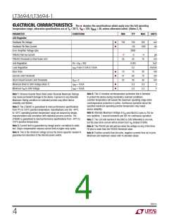
ELECTRICAL CHARACTERISTICS The l denotes the specifications which apply over the full operating
temperature range, otherwise specifications are at TA = 25°C, VIN = 12V, VBIAS = 3V, unless otherwise noted. (Notes 2, 9)
PARAMETER
CONDITIONS
MIN
TYP
MAX
UNITS
LDO Regulator
l
l
Feedback Pin Voltage
735
750
–50
2800
–3
765
mV
nA
Feedback Pin Bias Current
Error Amplifier Voltage Gain
TRK/SS Pull-Up Current
TRK/SS Threshold to Shut Down LDO
Line Regulation
–500
–2
35
–4
70
µA
mV
50
5V < V < 36V
0.025
0.5
15
%/V
mV/mA
mA
IN
Load Regulation
I
From 0.1mA to 10mA
DRV
l
l
Base Drive
10
47
22
20
70
Current Limit Threshold
Short-Circuit Current Limit Threshold
Minimum BIAS to DRV Voltage (Note 7)
60
mV
V
FB
= 0
26
30
mV
l
l
I
I
= 10mA
= 10mA
0.3
2.0
0.9
2.3
V
DRV
DRV
Minimum V to DRV Voltage
V
IN
Note 1: Stresses beyond those listed under Absolute Maximum Ratings
may cause permanent damage to the device. Exposure to any Absolute
Maximum Rating condition for extended periods may affect device
reliability and lifetime.
Note 2: The LT3694E is guaranteed to meet performance specifications
from 0°C to 125°C junction temperature. Specifications over the –40°C
to 125°C operating junction temperature range are assured by design,
characterization and correlation with statistical process controls. The
LT3694I is guaranteed to meet performance specifications from –40°C to
125°C junction temperature.
Note 5: This IC includes overtemperature protection that is intended
to protect the device during momentary overload conditions.
Junction temperature will exceed the maximum operating range when
overtemperature protection is active. Continuous operation above the
specified maximum operating junction temperature may impair
device reliability.
Note 6: Absolute Maximum Voltage at V and EN/UVLO pins is 70V for
IN
non-repetitive, 1 second transients and 36V for continuous operation.
Note 7: The LDO will function if the BIAS to DRV differential is not met,
but the base drive current will be drawn from V instead of BIAS.
IN
Note 3: Current limit is guaranteed by design and/or correlation to static
test. Slope compensation reduces current limit at higher duty cycles.
Note 8: The PGOOD pin will pull low when the voltage on any of the three
FB pins is lower than the PGOOD threshold value.
Note 4: This is the minimum voltage across the boost capacitor needed to
guarantee full saturation of the internal power switch.
Note 9: Positive currents flow into pins, negative currents flow out of pins.
Minimum and maximum values refer to absolute values.
36941fb
4

 Linear [ Linear ]