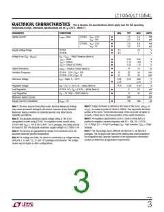
LT1054/LT1054L
PIN FUNCTIONS
is charging, the peak supply current will be approximately
capacitorof2µF,preferablytantalumorsomeotherlowESR
type is recommended. A larger capacitor may be desirable
in some cases, for example, when the actual input supply
is connected to the LT1054 through long leads, or when
the pulse current drawn by the LT1054 might affect other
circuitry through supply coupling.
equal to 2.2 times the output current. During the time that
C is delivering charge to C
the supply current drops
IN
OUT
to approximately 0.2 times the output current. An input
supply bypass capacitor will supply part of the peak input
current drawn by the LT1054 and average out the current
drawn from the supply. A minimum input supply bypass
APPLICATIONS INFORMATION
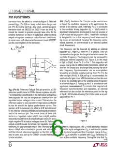
Theory of Operation
V1
V2
f
R
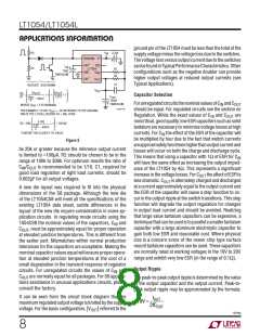
To understand the theory of operation of the LT1054, a re-
viewofabasicswitched-capacitorbuildingblockishelpful.
L
C1
C2
LT1054 • F03
In Figure 3 when the switch is in the left position, capaci-
tor C1 will charge to voltage V1. The total charge on C1
will be q1 = C1V1. The switch then moves to the right,
discharging C1 to voltage V2. After this discharge time
the charge on C1 is q2 = C1V2. Note that charge has been
transferred from the source V1 to the output V2. The
amount of charge transferred is:
Figure 3. Switched-Capacitor Building Block
R
EQUIV
V1
V2
1
fC1
R
L
C2
R
EQUIV
=
LT1054 • F04
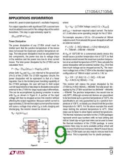
Figure 3. Switched-Capacitor Equivalent Circuit
∆q = q1 – q2 = C1(V1 – V2)
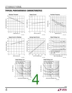
eventually be dominated by the 1/fC1 term and voltage
losses will rise.
If the switch is cycled f times per second, the charge
transfer per unit time (i.e., current) is:
Note that losses also rise as frequency increases. This is
caused by internal switching losses which occur due to
somefinitechargebeinglostoneachswitchingcycle.This
chargelossper-unit-cycle,whenmultipliedbytheswitching
frequency, becomes a current loss. At high frequency this
loss becomes significant and voltage losses again rise.
I = (f)(∆q) = (f)[C1(V1 – V2)]
To obtain an equivalent resistance for the switched-
capacitor network we can rewrite this equation in terms
of voltage and impedance equivalence:
V1– V2 V1– V2
1/ fC1 REQUIV
I=
=
The oscillator of the LT1054 is designed to run in the
frequency band where voltage losses are at a minimum.
A new variable R is defined such that R
= 1/fC1.
EQUIV
EQUIV
Thus the equivalent circuit for the switched-capacitor
network is as shown in Figure 4. The LT1054 has the same
switching action as the basic switched-capacitor building
block.Eventhoughthissimplificationdoesn’tincludefinite
switchon-resistanceandoutputvoltageripple, itprovides
anintuitivefeelforhowthedeviceworks.
Regulation
T
he error amplifier of the LT1054 servos the drive to the
PNPswitchtocontrolthevoltageacrosstheinputcapaci-
tor (C ) which in turn will determine the output voltage.
IN
Using the reference and error amplifier of the LT1054,
an external resistive divider is all that is needed to set
the regulated output voltage. Figure 5 shows the basic
regulator configuration and the formula for calculating
the appropriate resistor values. R1 should be chosen to
1954lfg
These simplified circuits explain voltage loss as a function
of frequency (see Typical Performance Characteristics).
As frequency is decreased, the output impedance will
7

 Linear [ Linear ]