LT1054/LT1054L
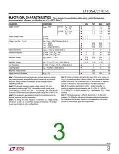
ELECTRICAL CHARACTERISTICS The l denotes the specifications which apply over the full operating
temperature range, otherwise specifications are at TA = 25°C. (Note 7)
PARAMETER
CONDITIONS
= 0mA
MIN
TYP
MAX
UNITS
l
l
Supply Current
I
LT1054:
V
IN
V
IN
= 3.5V
= 15V
2.5
3.0
4.0
5.0
mA
mA
LOAD
l
l
LT1054L: V = 3.5V
2.5
3.0
4.0
5.0
mA
mA
IN
V
= 7V
IN
l
l
Supply Voltage Range
LT1054
LT1054L
3.5
3.5
15
7
V
V
Voltage Loss (V – |V |)
C
= C
= 100µF Tantalum (Note 4)
OUT
IN
OUT
IN
l
l
l
I
I
I
= 10mA
0.35
1.10
1.35
0.55
1.60
1.75
V
V
V
OUT
OUT
OUT
= 100mA
= 125mA (LT1054L)
l
Output Resistance
10
15
Ω
∆I
OUT
= 10mA to 100mA (Note 5)
l
l
Oscillator Frequency
LT1054: 3.5V ≤ V ≤ 15V
15
15
25
25
40
35
kHz
kHz
IN
LT1054L: 3.5V ≤ V ≤ 7V
IN
Reference Voltage
I
= 60µA, T = 25°C
2.35
2.25
2.50
2.65
2.75
V
V
REF
J
l
Regulated Voltage
Line Regulation
Load Regulation
V
= 7V, T = 25°C, R = 500Ω (Note 6)
–4.70
–5.00
5
–5.20
25
V
mV
mV
mA
µA
IN
J
L
l
l
LT1054: 7V ≤ V ≤ 12V, R = 500Ω (Note 6)
IN
L
V
IN
= 7V, 100Ω ≤ 500Ω (Note 6)
10
50
Maximum Switch Current
300
100
l
Supply Current in Shutdown
V
= 0V
200
PIN1
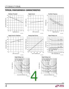
Note 5: Output resistance is defined as the slope of the curve, (∆V
OUT
portion of the curve. The incremental slope of the curve will be higher at
currents <10mA due to the characteristics of the switch transistors.
vs
Note 1: Stresses beyond those listed under Absolute Maximum Ratings
may cause permanent damage to the device. Exposure to any Absolute
Maximum Rating condition for extended periods may affect device
reliability and lifetime.
OUT
∆I ), for output currents of 10mA to 100mA. This represents the linear
Note 6: All regulation specifications are for a device connected as a
positive-to-negative converter/regulator with R1 = 20k, R2 = 102.5k,
Note 2: The absolute maximum supply voltage rating of 16V is for
unregulated circuits using LT1054. For regulation mode circuits using
C1 = 0.002µF, (C1 = 0.05µF S package) C = 10µF tantalum, C
= 100µF
LT1054 with V
≤ 15V at Pin 5 (Pin 11 on S package), this rating may be
IN
OUT
OUT
tantalum.
increased to 20V. The absolute maximum supply voltage for LT1054L is 7V.
Note 7: The S8 package uses a different die than the H, J8, N8 and S
packages. The S8 device will meet all the existing data sheet parameters.
See Regulation and Capacitor Selection in the Applications Information
section for differences in application requirements.
Note 3: The devices are guaranteed by design to be functional up to the
absolute maximum junction temperature.
Note 4: For voltage loss tests, the device is connected as a voltage inverter,
with pins 1, 6, and 7 (3, 12, and 13 S package) unconnected. The voltage
losses may be higher in other configurations.
1954lfg
3

 Linear [ Linear ]