LT1054/LT1054L
APPLICATIONS INFORMATION
wheredV=peak-to-peakrippleandf=oscillatorfrequency.
where:
For output capacitors with significant ESR a second term
mustbeaddedtoaccountforthevoltagestepattheswitch
transitions. This step is approximately equal to:
V ≈ V – [(LT1054 Voltage Loss)(1.3) + |VOUT|]
X
IN
and I
= maximum required output current. The factor
OUT
of 1.3 will allow some operating margin for the LT1054.
(2I )(ESR of C
)
OUT
OUT
For example: assume a 12V to –5V converter at 100mA
outputcurrent.Firstcalculatethepowerdissipationwithout
an external resistor:
Power Dissipation
The power dissipation of any LT1054 circuit must be
limited such that the junction temperature of the device
does not exceed the maximum junction temperature rat-
ings. The total power dissipation must be calculated from
two components, the power loss due to voltage drops
in the switches and the power loss due to drive current
losses. The total power dissipated by the LT1054 can be
calculated from:
P = (12V – |–5V|)(100mA) + (12V)(100mA)(0.2)
P = 700mW + 240mW = 940mW
At θ of 130°C/W for a commercial plastic device this
JA
would cause a junction temperature rise of 122°C so that
the device would exceed the maximum junction tempera-
ture at an ambient temperature of 25°C. Now calculate the
power dissipation with an external resistor (R ). First find
X
how much voltage can be dropped across R . The maxi-
X
P ≈ (V – |VOUT|)(I ) + (V )(I )(0.2)
IN
OUT
IN OUT
mum voltage loss of the LT1054 in the standard regulator
where both V and V
are referred to the ground pin
configuration at 100mA output current is 1.6V, so:
IN
OUT
(Pin 3) of the LT1054. For LT1054 regulator circuits, the
power dissipation will be equivalent to that of a linear
regulator. Due to the limited power handling capability of
the LT1054 packages, the user will have to limit output
currentrequirementsortakestepstodissipatesomepower
external to the LT1054 for large input/output differentials.
This can be accomplished by placing a resistor in series
V = 12V – [(1.6V)(1.3) + |–5V|] = 4.9V and
X
R = 4.9V/(4.4)(100mA) = 11Ω
X
This resistor will reduce the power dissipated by the
LT1054 by (4.9V)(100mA) = 490mW. The total power dis-
sipated by the LT1054 would then be (940mW – 490mW)
= 450mW. The junction temperature rise would now be
only 58°C. Although commercial devices are guaranteed
to be functional up to a junction temperature of 125°C, the
specifications are only guaranteed up to a junction tem-
perature of 100°C, so ideally you should limit the junction
temperature to 100°C. For the above example this would
mean limiting the ambient temperature to 42°C. Other
steps can be taken to allow higher ambient temperatures.
The thermal resistance numbers for the LT1054 packages
represent worst-case numbers with no heat sinking and
still air. Small clip-on type heat sinks can be used to lower
the thermal resistance of the LT1054 package. In some
systems there may be some available airflow which will
helptolowerthethermalresistance. WidePCboardtraces
from the LT1054 leads can also help to remove heat from
the device. This is especially true for plastic packages.
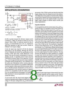
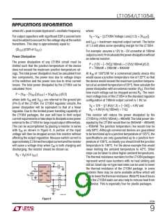
with C as shown in Figure 6. A portion of the input
IN
voltage will then be dropped across this resistor without
affecting the output regulation. Because switch current is
approximately2.2timestheoutputcurrentandtheresistor
will cause a voltage drop when C is both charging and
IN
discharging, the resistor should be chosen as:
R = V /(4.4 I
)
X
X
OUT
V
IN
+
FB/SHDN
V
R
X
+
CAP
OSC
+
LT1054
R1
R2
C1
C
IN
GND
V
REF
–
CAP
V
OUT
V
OUT
C
OUT
+
LT1054 • F06
Figure 6
1954lfg
9

 Linear [ Linear ]