LT1054/LT1054L
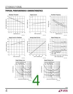
TYPICAL PERFORMANCE CHARACTERISTICS
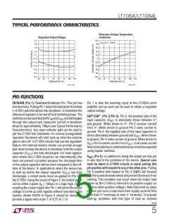
Reference Voltage Temperature
Coefficient
Regulated Output Voltage
–4.7
–4.8
100
80
V
REF
AT 0 = 2.500V
–4.9
60
–5.0
40
–5.1
20
–11.6
–11.8
–12.0
–12.2
–12.4
–12.6
0
–20
–40
–60
–80
–100
–50
0
25
50
75 100 125
–50
0
25
50
75 100 125
–25
–25
TEMPERATURE (°C)
TEMPERATURE (°C)
LT1054 • TPC09
LT1054 • TPC10
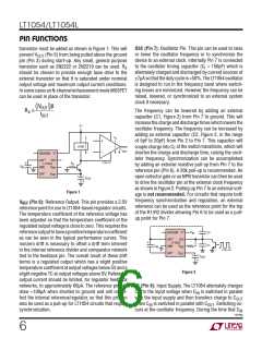
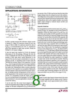
PIN FUNCTIONS
FB/SHDN (Pin 1): Feedback/Shutdown Pin. This pin has
twofunctions.PullingPin1belowtheshutdownthreshold
(≈0.45V) puts the device into shutdown. In shutdown the
reference/regulator is turned off and switching stops. The
switchesaresetsuchthatbothC andC aredischarged
Pin 1 is also the inverting input of the LT1054’s error
amplifier and as such can be used to obtain a regulated
output voltage.
+
–
CAP /CAP (Pin 2/Pin 4): Pin 2, the positive side of the
+
IN
OUT
input capacitor (C ), is alternately driven between V
IN
through the output load. Quiescent current in shutdown
drops to approximately 100µA (see Typical Performance
Characteristics). Any open-collector gate can be used to
put the LT1054 into shutdown. For normal (unregulated)
operation the device will start back up when the external
gate is shut off. In LT1054 circuits that use the regulation
feature, the external resistor divider can provide enough
pull-down to keep the device in shutdown until the output
+
and ground. When driven to V , Pin 2 sources current
+
from V . When driven to ground Pin 2 sinks current to
ground. Pin 4, the negative side of the input capacitor, is
driven alternately between ground and V . When driven
OUT
to ground, Pin 4 sinks current to ground. When driven to
V
Pin 4 sources current from C . In all cases current
OUT
OUT
flowintheswitchesisunidirectionalasshouldbeexpected
using bipolar switches.
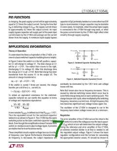
capacitor (C ) has fully discharged. For most applica-
OUT
V
OUT
(Pin 5): In addition to being the output pin this pin
tions where the LT1054 would be run intermittently, this
does not present a problem because the discharge time
of the output capacitor will be short compared to the off-
time of the device. In applications where the device has
is also tied to the substrate of the device. Special care
must be taken in LT1054 circuits to avoid pulling this
pin positive with respect to any of the other pins. Pulling
Pin 5 positive with respect to Pin 3 (GND) will forward
biasthesubstratediodewhichwillpreventthedevicefrom
starting. This condition can occur when the output load
driven by the LT1054 is referred to its positive supply (or
to some other positive voltage). Note that most op amps
present just such a load since their supply currents flow
to start up before the output capacitor (C ) has fully
OUT
discharged, a restart pulse must be applied to Pin 1 of
the LT1054. Using the circuit of Figure 5, the restart signal
can be either a pulse (t > 100µs) or a logic high. Diode
p
coupling the restart signal into Pin 1 will allow the output
voltage to come up and regulate without overshoot. The
resistor divider R3/R4 in Figure 5 should be chosen to
provide a signal level at pin 1 of 0.7V to 1.1V.
+
–
from their V terminals to their V terminals. To prevent
start-up problems with this type of load an external
1954lfg
5

 Linear [ Linear ]